In order to ensure that the chip can work reliably, the hardware power supply design must meet the power-up sequence and power-down timing of the chip manual. Otherwise, the current may be too large, abnormal startup, or even damage the processor when the product is used. This article uses i.MX6UL as an example to introduce the design of the power-up sequence.
First, i.MX6UL power up and down timing requirements
Power up sequence:
1. VDD_SNVS_IN must be powered on alone (shorted) together with VDD_HIGH_IN, after which other supplies can be powered up.
2. If you are using a coin cell battery for VDD_SNVS_IN, be sure to connect it before turning on any other power.
3. VDD_HIGH_IN should be turned on before VDD_SOC_IN.
Power down sequence:
1. VDD_SNVS_IN must be powered off either alone or together (shorted) with VDD_HIGH_IN before all other power supplies must be powered down.
2. If you are using a coin cell battery to power VDD_SNVS_IN, make sure to remove any other power supplies after removing them.
Second, i.MX6UL power management unit - PMU

Third, the main points of analysis
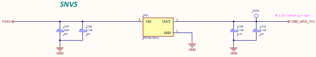
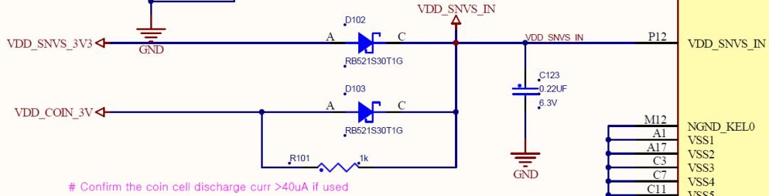
According to the figure of the i.MX6UL power management unit, the VDD_SNVS_IN pin that is the first power supply is used as the input of the internal LDO_SNVS, and the output voltage VDD_SNVS_CAP is the power supply to the SNVS module and the real-time clock module OSC32K. If it is necessary to maintain the RTC in case of power failure, then VDD_SNVS_IN needs to be powered separately, otherwise it can be connected with VDD_HIGH_IN. The coin cell scheme can be reserved in the VDD_SNVS_IN design to meet the application requirements for power-down keeping the real-time clock, but if a button cell is used to power VDD_SNVS_IN, make sure to connect it before turning on any other power.
According to the previous power-up sequence, VDD_HIGH_IN can be first powered on together with the VDD_SNVS_IN power supply. In the case where the system needs to be powered down to maintain the real-time clock, since VDD_HIGH_IN consumes a relatively large amount of power, it is necessary to separately process the two power supplies while maintaining the real-time clock. The power supply module that is powered on can be enabled using the control signal PMIC_ON_REQ in the SNVS power domain to achieve the power-up timing requirements, as shown in the following figure.
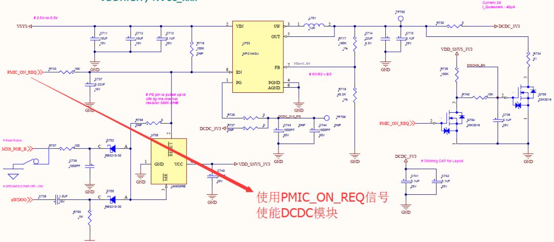
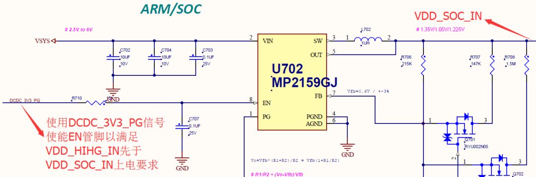
According to the power-up sequence, the VDD_SOC_IN power-up sequence is later than VDD_HIGH_IN. Therefore, in the circuit design, the VDD_HIGH_IN power supply chip control signal can be used to enable the VDD_SOC_IN power supply. As shown in the following figure, the PG signal using the VDD_HIGH_IN power supply chip enables VDD_SOC_IN. Power supply chip enable pins.
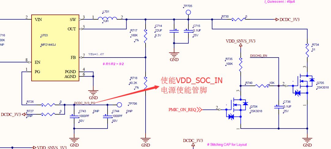
Use the DCDC_3V3_PG to control the VDD_SOC_IN power enable pin to meet the VDD_HIGH_IN power-on VDD_SOC_IN requirement as shown in the following figure.
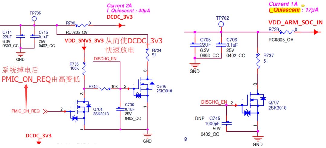
According to power-down timing requirements, the power-off priority order can be as long as the last power-down of VDD_SNVS_IN is satisfied. The corresponding controllable power-down circuit is added to the design to enable the downstream filter capacitor to be quickly discharged to achieve the power-down sequence. The following figure shows the DCDC_3V3 power-down circuit, and DCDC_3V3 supplies VDD_HIGH_IN. Working principle: After the system is powered off, PMIC_ON_REQ changes from high level to low level, so that the DISCHG_EN signal goes high, so that the DCDC_3V3 current is turned on to GND through the resistor R734 and the MOS transistor Q705. The VDD_SOC_IN voltage passes through the DISCHG_EN signal. Control MOS tube Q707 fast power down, as shown below.
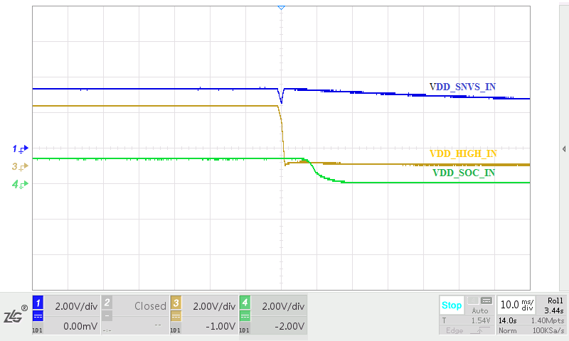
The i.MX6UL power-up timing waveform is shown below, where VDD_SOC_IN is the core voltage - 1.35V.

i.MX6UL power down timing waveform as shown below.
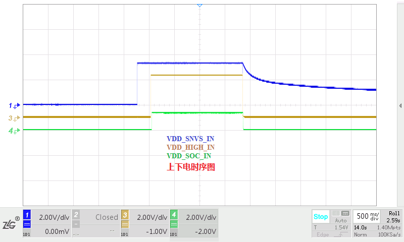
The complete waveform diagram of the power up and down timing is shown in the figure below.
Fourth, the conclusion
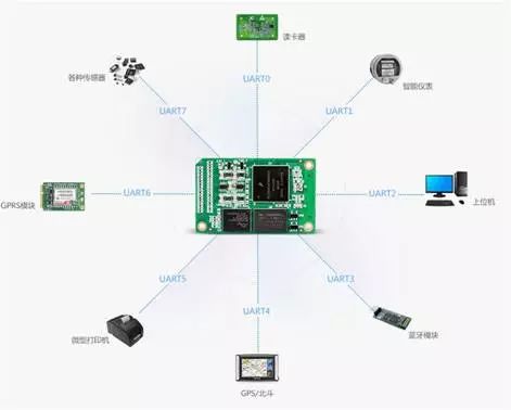
The M6G2C uses the i.MX6UL processor to meet the strict power-up and power-down sequence of the chip manual. It is an industrial control core board that uses a Freescale Cortex-A7 528MHz clocked processor to bring lower power consumption with an advanced power management architecture. Standard 8 UART, 2 USB OTG, 2 CAN-Bus, 2 Ethernet and other interfaces; 128/256MB DDR3 and 128/256MB NAND Flash, hardware watchdog as standard; passed strict EMC and high and low temperature test, Ensure that the core board works stably under harsh conditions.
Laptop Holder Vertical Double,Laptop Holder Vertical Stand,Laptop Holder Vertical Adjustable,Laptop Holder Vertical Desk,etc.
Shenzhen Chengrong Technology Co.ltd is a high-quality enterprise specializing in metal stamping and CNC production for 12 years. The company mainly aims at the R&D, production and sales of Notebook Laptop Stands and Mobile Phone Stands. From the mold design and processing to machining and product surface oxidation, spraying treatment etc ,integration can fully meet the various processing needs of customers. Have a complete and scientific quality management system, strength and product quality are recognized and trusted by the industry, to meet changing economic and social needs .

Laptop Holder Vertical Double,Laptop Holder Vertical Stand,Laptop Holder Vertical Adjustable,Laptop Holder Vertical Desk
Shenzhen ChengRong Technology Co.,Ltd. , https://www.dglaptopstandsupplier.com