This paper introduces an ultrasonic motor motion control device designed by DSP56F801, a DSP chip for motion control. Since the ultrasonic motor needs to adopt two-phase four-way symmetric PWM signal to realize the drive control, and the DSP chip cannot directly generate the required PWM signal, the software method takes up a lot of DSP calculation time, so the programmable logic device is designed. Symmetric PWM signal generator for CPLD). The signal generator can realize the duty cycle and phase difference adjustment of the output two-phase PWM control signal under the control of the DSP. At the same time, the programmable oscillator LTC6903 with SPI interface is used to realize the frequency adjustment of the PWM control signal under the control of the DSP. . It can be seen that in order to realize the DSP control of the duty cycle, phase difference and frequency of the PWM control signal, it is necessary to implement the control information transmission between the DSP and the CPLD and the LTC6903 by using appropriate communication methods. The DSP56F801 chip has an SPI communication port. Based on the analysis of SPI data transmission timing relationship, this paper designs and implements multi-SPI interface communication based on CPLD.
1 Working principle
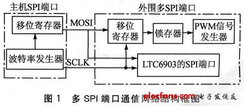
The SPI is a synchronous protocol interface, and all transmissions refer to a common clock. A master chip can be connected to multiple slave chips on the same SPI port. At this time, the master selects the slave device by triggering the chip select input pin of the slave device, and the slave device that is not selected will not participate in the SPI transmission. The SPI master uses four signals: master output/slave input (MOSI), master input/slave output (MISO), serial clock signal SCLK, and peripheral chip select signal (SS). Both the host and peripherals contain a serial shift register, and the master initiates a transfer by writing a byte to its SPI serial shift register. The register transfers the byte to the slave device through the MOSI pin, and the slave device also returns the contents of its own shift register to the host through the MISO signal line. Thus, the contents of the two shift registers are swapped. The write and read operations of the peripheral are done synchronously, so SPI becomes a very effective serial communication protocol. The block diagram of the communication network of the SPI port is shown in Figure 1. In order for the signal generator to output two-phase four-way PWM waves of adjustable frequency, voltage regulation and phase modulation output, the DSP needs to output parameters to the CPLD circuit. The transfer of these four control parameters is implemented in a small communication network. In this network, the SPI of the DSP only performs the write operation of the data output port, that is, the output voltage control word, the phase control word, and the frequency control word. Data flow: The host DSP transfers data to the CPLD. When transmitting data, the data is output on the MOSI pin, and the data is synchronously shifted output under the action of the clock signal. Since no slave data is required to be sent back to the host, the host ends the transfer after the data transfer ends. Since there is no acknowledge signal when the SPI port is working, and the data does not need to be verified when transmitting, it is required that the data transmission and reception of the master and slave devices must fully comply with the set SPI timing requirements, otherwise the data transmission will be wrong.
2 CPLD-based serial SPI design
2.1 shift register design
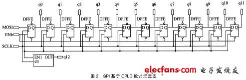
This design is a 12-bit SPI serial receive port. The shift register in Figure 1 is composed of 12 D flip-flops and 1 counter, which implements shift reception and serial-to-parallel conversion. During the transfer, the shift register and counter are enabled first to initiate the transfer and the counter starts counting. When counting to 16, the carry terminal outputs a high-level pulse of pulse width for data latching, and its circuit is as shown in FIG. 2.
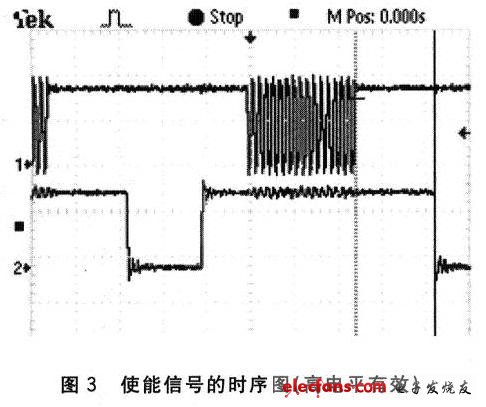
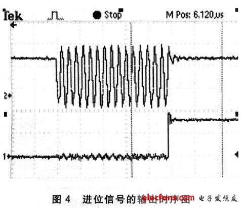
In order to ensure the correct timing, the output timing of the enable signal and the counter carry pulse is measured, as shown in Figure 3 and Figure 4. The hexadecimal counter uses the rising edge count. When the 16th rising edge comes, it jumps to the high level to ensure the correct receiving and latching of the data.
Coupletech Co., Ltd., manufactures, develops and markets a variety of optical crystals which are widely used in the field of optoelectronics, Coupletech product line consists of all kinds of crystal: laser crystals including Nd:YVO4, Nd:YAG, Diffusion Bonded Composite Crystal, Cr:YAG, Nd:YLF etc.; Nonlinear optical ( NLO ) crystals, including KTP, KTA, BIBO, LBO, BBO, DKDP, KDP, LiNbO3 crystal, etc.; Fluoride crystals including CaF2, BaF2, MgF2; Periodically poled crystals: PPLN crystal, MgO:PPLN crystal. We combine high and strict quality manufacturing to supply our products at the most attractive price. We also provide Ti: Sapphire, TGG, AGS, ZGP and other crystals for laser and telecom industries.
Coupletech's Optical Crystal combined with our wide experience and deep technology, we are able to deliver the optimum solution for your applications. We are flexible in customized products and features in high surface accuracy, high surface quality, high flatness. We are also well experienced in the high laser damage threshold AR coatings and HR coatings.
Optical Crystal
Optical Crystal,Laser Crystal,Nonlinear Optical Crystal,Magneto-Optic Crystal
Coupletech Co., Ltd. , https://www.coupletech.com