Circuit function and advantage
In a multi-channel DAC system, all outputs can be monitored from a single point, which is very advantageous for troubleshooting and diagnostic analysis. The circuit described in this paper utilizes a single-channel SAR ADC to achieve output channel monitoring of a multi-channel DAC.
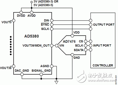
Figure 1: Typical channel monitoring circuit
Circuit description
The circuit shown in Figure 1 utilizes a 40-channel, 14-bit DACAD5380 internal multiplexer that allows all 40 output channels to be routed separately to a single output (MON_OUT) pin and then monitored by an external ADC (AD7476). This method utilizes much less circuitry than the circuitry required to monitor each channel individually.
The AD5380 is a complete 40-channel, 14-bit DAC that operates from a single supply. All 40 channels have a rail-to-rail on-chip output amplifier. The AD5380 has built-in channel monitoring, which is implemented by a multiplexer that is addressed via the serial interface. Any channel output can be routed to the monitor output (MON_OUT) pin for monitoring with an external ADC. To route any channel to MON_OUT, the channel monitoring function must first be enabled in the control register. The microcontroller or processor can select the output channel to monitor through its serial output port and then read the ADC converted data through its serial input port.
The AD5380-3 operates from a 3 V supply and the AD5380-5 operates from a 5 V supply. The AD7476 ADC provides 12-bit resolution, operates from a single 2.35 V to 5.25 V supply, integrates a voltage reference, features low power, small size and serial interface, throughput rates up to 1 MSPS, and a 6-pin SOT -23 package. The slew rate is determined by SCLK and has a throughput rate of up to 1 MSPS.
The AD5380 and AD7476 must have a large enough supply bypass capacitor of 10 μF in parallel with the 0.1 μF capacitor on each supply pin, as close as possible to the package, preferably directly opposite the device (this state is not shown on the schematic). The 10 μF capacitor is a bead type capacitor.
A 0.1 μF capacitor must have low effective series resistance (ESR) and low effective series inductance (ESL), such as a common ceramic type capacitor that provides a low impedance ground path at high frequencies to handle transient currents caused by internal logic switching.
The power traces should be as wide as possible to provide a low impedance path and reduce the glitch on the power line. Fast switching signals, such as clocks, must be shielded by ground lines to avoid radiating noise to other devices on the board and should never be close to analog signals. Deploying a ground line between the SDATA line and the SCLK line helps to reduce crosstalk between the two (not required on a multi-layer board because it has a separate ground plane; however, the ground line helps separate the different lines). Avoid overlapping digital signals with analog signals. The traces on opposite sides of the board should be perpendicular to each other to help reduce the feedthrough effect on the board. Microstrip line technology is recommended, but this technology may not always work for double-sided boards. With this technique, the component side of the board is dedicated to the ground plane and the signal traces are routed to the solder side. The board requires at least 4 layers for optimal layout and performance: a ground plane, a power plane, and two signal layers.
Common changes
Pin-compatible products of the AD7476 can be used in surveillance applications that accept lower resolution conversions. The AD7477 provides 10-bit resolution and the AD7478 provides 8-bit resolution.
Ral7035 Control Box,Q235 Control Box,304Ss Control Box,316Ss Control Box
Nantong Double Star Automation Equipment Co., Ltd. , https://www.nt-doublestar.com