Embedded emulator
This article refers to the address: http://
Designed for complex automotive electronics applications, the MC33993, MC33887, and MC33888 devices offer advanced performance and diagnostics solutions.
Complex multi-pin MCUs often cause development problems. The MC9S12DP256 provides a single-line background debug interface that makes it easy to perform extensive debugging in an automotive environment without the difficulties common to using traditional circuit-embedded emulators. This interface can also be used to program the main flash memory at the end of the line and even to perform reprogramming operations in the car.
Modern automotive microcontrollers often use flash memory to store the main operating program. The best way to program the flash is to program the main program into the complete electronic control module after final assembly. This method can effectively avoid risks and delays compared to programming the main program into the MCU by a third party before module assembly. Time. Programming the main program into the MCU via a simple serial interface is done after the module is assembled and is typically executed during the final test. Some manufacturers use inexpensive stand-alone programmers to do this, while others integrate programming operations into test equipment at the end of the line.
Motorola's related devices provide a single-line background debug interface for flash programming, verification, and general debugging operations. When the device is operating normally, the serial communication pin is pulled high during reset, so the background system is not activated. When a programmer or debug system is connected to this pin, the pin is pulled low on reset, forcing the MCU into active background mode instead of launching the application. In order to facilitate debugging, a host system can be connected to the target MCU system during normal operation of the device, thereby monitoring the flash memory or register contents without interfering with the operation of the device. The connected debug system can also replace the MCU's control to read and write CPU registers, set hardware breakpoints, or track a single instruction.
A traditional circuit-embedded emulator typically requires between 30 and 40 connections to the target system, while the background debug interface requires only two to four connections. A single BKGD communication signal and public ground are required. Increasing the reset signal makes it easier for the host to force and control the system reset. In some cases, increasing VDD allows the debug fixture to "steal" power from the target system. This simple interface provides automotive electronics designers with the ability to debug access to MCUs installed in the sports car's electronic control module. Many problems can only be discovered when the car is traveling under normal road conditions.
Memory programming
The most important factors associated with flash programming are speed and convenience. The programming speed depends on the programming time of the flash cell and the data transfer speed from the programmer to the target MCU. Of course, there are other factors, such as the time to erase the array before programming, to verify the success of the programming operation. The MC9S12DP256 programs any 16-bit word for 45ms, but a burst programming operation allows programming of any additional word in the same bank of 32-word flashes at 20ms. In theory, the single-line background debug interface can transfer a word of information within 27ms, which is slightly slower than the actual programming time of the flash. Actual programming also requires additional task overhead, such as verification overhead. The independent programmer tool SCBDMPGMR12 can erase, program and verify 256KB of flash memory in less than 10s.
Verification is one of the important factors that generate overhead. Retransmitting all the data to achieve word-to-word verification will double the programming time. A quick way to do this is to perform a CRC calculation when the data is programmed into the flash and then reread the flash content to verify the CRC value after the entire flash programming is complete. This operation is fully possible at bus speed and there is no need to retransmit data.
Separating the data-to-target transfer so that it is completed before the data is programmed into the flash also doubles the programming time. A better approach is to extend the data transfer in parallel with the programming operation. In general, the programming algorithm is sent to the target MCU first, which facilitates management of the received data and sends the data to the RAM buffer, and then controls the erase and program operations. The programming algorithm utilizes two data buffers to receive data to be programmed into the flash. When the first buffer is full of data, the programming algorithm begins programming the data into flash and the new data is loaded into the second buffer. The background interface can be used to receive data and write them to RAM. This operation does not interfere with the operation of the target CPU because the CPU reads data from another buffer and programs it into the flash.
The flash memory in the MC9S12DP256 is divided into four independent 64KB blocks, so the erase and program operations can be performed independently on these four blocks. In the case of flash programming based on background debugging, since the data transfer speed is slightly slower than the average word programming speed of the flash memory, it is impractical to attempt to interleave the programming operation of the independent array, but perform batch rubbing on all 4 blocks in parallel. It is feasible except for the operation.
Background access provides an extremely convenient way for first-time flash programming, but some users still want to use other system buses such as CAN bus, J1850 bus or serial interface bus to perform all field reprogramming operations. This can be done easily by including the appropriate boot loader program in the main application. In order to respond to certain special codes from a bus in a finished car, the boot loader should be able to erase the flash and accept new programming data.
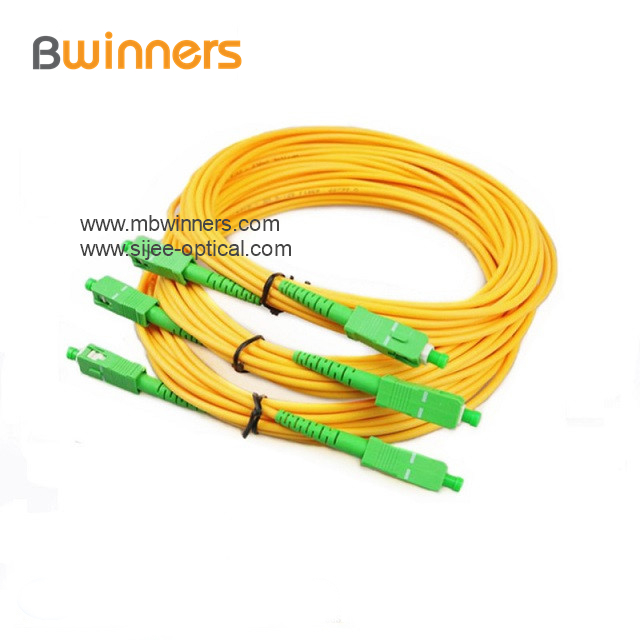
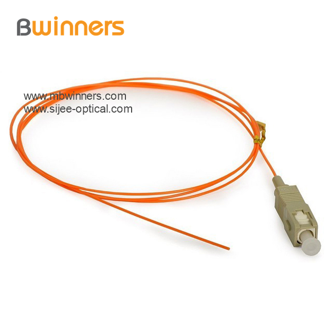
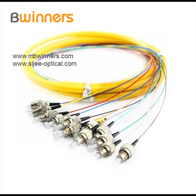
Fiber patchcord and pigtails are essential passive components for FTTH ODN connectivity; Bwinners offers different types of fiber connectivity cables with fully customized connectors, main products including Fiber Patchcord, Fiber Pigtail, Fiber Bunchy Cable, Ribbon Fiber Cable, Fiber Breakout Cable, Fiber Drop Cable, Fiber MPO Patchcord, Optical Cable Pigtail, Fiber Optic Ribbon Pigtail, Fiber Optic Patch Cord, Optical Fiber Pigtail .etc.
Technical specifications:
|
Pigtail Connector |
PC (SM) |
UPC (SM) |
APC (SM) |
MM |
|
Return Loss (dB) |
≥45 |
≥50 |
≥60 |
≥35 |
|
Insertion Loss (dB) |
≤0.2 (max≤0.3) |
|||
|
Repeatability (dB) |
≤0.1 |
|||
|
Durability(1/Matings) |
≥500 |
|||
|
Operation Temperature (°C) |
-25~+70 |
|||
|
Tensile Strength (N) |
≥90 (Φ3.0), ≥70 (Φ2.0), Φ0.9 |
|||
|
Fiber |
9/125um, 50/125um,62.5/125um,ect |
|||
|
Diameter |
0.9mm 2.0mm, 3.0mm etc |
|||
|
Cable material |
PVC, LSZH |
|||
|
Cores |
Simplex, duplex, 4cores, 6cores, 8cores, 12cores etc |
|||
Features:
1. Good durability
2. Good exchangeability
3. High temperature stability
4. Low insertion loss and back reflection loss
5. Superior Quality Standard PC/UPC/APC Polishing
6. Standard: Telcordia GR-326-CORE, TIA/EIA and IEC
7. The patch cord can be customized according to customer`s specific requirements
Applications:
1. Optical fiber communication system
2. Telecommunication network
3. LANs and WANs
4. FTTX, LAN, PON & Optical CATV, Local ring net
5. Optical fiber test equipment
6. Optical fiber sensor
7. Industry and military application


Free samples are available for your testing.
Optical Cable Pigtail,Fiber Optic Ribbon Pigtail,Fiber Optic Patch Cord,Optical Fiber Pigtail
Sijee Optical Communication Technology Co.,Ltd , https://www.sijee-optical.com