Introduction: Speaking of the difficulty of switching power supply, the problem of PCB layout is not very difficult, but if it is to produce a sophisticated PCB, it must be one of the difficulties in switching power supply. (PCB design is not good, may lead to no matter how to debug parameters Debugging is not an alarmist thing. The reason is that there are many factors that are considered when PCB layout, such as: electrical performance, process routes, safety requirements, EMC impact, etc.; among the factors considered, electrical is the most Basic, but EMC is the most difficult to find out, the bottleneck of progress in many projects lies in EMC issues; the next from the 22nd direction to share PCB layout and EMC.
First, the EMI circuit of the PCB design can be easily carried out by the cooked circuit
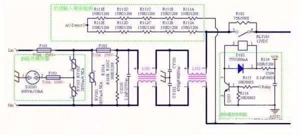
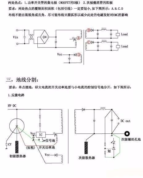
The above circuit can imagine the impact of EMC, the input filter is here; anti-lightning pressure sensitive; to prevent the impact of the current resistance R102 (cooperate with the relay to reduce the loss); the key to the difference between the X capacitor and Inductor coupled with the filtered Y capacitor; there are also fuses that affect the layout of the safety regulations; each device here is critical, to savor the function and role of each device. The design of the circuit must consider the EMC severity level design, such as setting several levels of filtering, the number of Y capacitors, and the location. The selection of pressure-sensitive sizes is closely related to our needs for EMC. We welcome everyone to discuss EMI circuits that appear to be simple and in fact each component contains profound truth. Second, circuit and EMC: (most familiar with the main topology, look at the key areas in the circuit that contains the EMC mechanism)
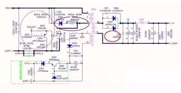
The circuit in the above figure is circled in several parts: it is very important for EMC (note that the green part is not). For example, radiation is known as electromagnetic field radiation is spatial, but the basic principle is the change of magnetic flux. The magnetic flux involves the effective cross-sectional area of ​​the magnetic field. , which is the corresponding loop in the circuit. Electric currents can produce magnetic fields that produce stable magnetic fields that cannot be converted into electric fields; but changing electric currents produce changing magnetic fields, and changing magnetic fields can generate electric fields (in fact, this is the famous Maxwell equation I use in the popular language). The same electric field can produce a magnetic field. Therefore, we must pay attention to those places where there is a switch state, that is, one of the sources of EMC. Here is one of the sources of EMC. (Of course, one of them will be mentioned later.) For example, a dashed-line loop in the circuit is the opening of the switch. And the loop that shuts off, not only when the circuit is designed, the switching speed can be adjusted to influence EMC, but also the area of ​​the routing loop of the layout board has an important influence! The other two loops are the absorption loop and the rectification loop. Third, PCB design and EMC correlation 1. PCB loop impact on EMC is very important, such as flyback main power loop, if too much, then radiation will be very poor. 2. Filter line effect, the filter is used to filter out the interference, but if the PCB alignment is not good, the filter may lose the effect it should have. 3. In the structure part, the poor design of the radiator will affect the grounding of the shielded version, etc. 4. The sensitive part is too close to the source of the interference. For example, the EMI circuit is very close to the switch tube, which will inevitably lead to poor EMC and need to be clearly defined. Isolated area. 5. RC absorption circuit traces. 6. Y capacitor ground and trace, as well as the location of the Y capacitor is also critical and so on! and many more. Think of these things first, and follow-up will discuss them in concrete terms, starting with an introduction. Here is a small example:
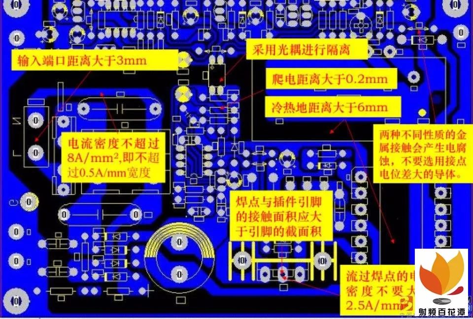
As shown in the dashed box in the figure above, the X capacitor pin traces are retracted. We can learn how to make the capacitor pin traces (using squeeze current traces). In this way, the filtering effect of the X-capacitor can be optimal. Fourth, the preparation of PCB design matters: (prepared, before design can be robust, to avoid design overthrow again) generally have the following aspects, are their own design process will consider, all of the content has nothing to do with other tutorials , is just a summary of their own experience. 1. Appearance structure size, including positioning holes, air flow direction, input and output sockets, need to match with the customer system, also need to communicate with the customer on the assembly of the problem, limit height and so on. 2. Safety certification, what kind of product certification, which places do the basic insulation creepage distance to stay enough, and where to do to strengthen insulation distance or slot. 3. Package design: There is no special period, such as custom package preparation. 4. Process route selection: single-panel dual-panel selection, or multi-layer board, based on schematics and board size, cost and other comprehensive assessment. 5. Other special requirements of the customer. The structural process will be relatively more flexible, safety regulations are still relatively fixed, what certifications are made, what safety standards are adopted, and of course there are some safety regulations that are common to many standards, but there are also some special products such as medical care that are more stringent. In order not to dazzle the friends of the new entry engineers, the following is a list of common products, the following is the specific layout requirements for the IEC60065 summary, for safety regulations need to keep in mind that the specific product will be targeted to deal with: 1. The distance between the input fuse parts and safety requirements is greater than 3.0MM, the actual layout is in accordance with 3.5MM (Simplified before the fuse in accordance with 3.5MM creepage distance, followed by 3.0MM creepage distance) 2. Before and after rectifier bridge safety requirements 2.0 MM, cloth board in accordance with 2.5MM. 3. After rectification safety regulations generally do not require, but according to the actual voltage size between high and low pressure to stay away from the habit of 400V high pressure to stay above 2.0MM. 4. The safety requirements for primary and secondary systems are 6.4 MM (electrical clearance), and the creepage distance is 7.6 MM. (Note that this is related to the actual input voltage, you need to look up the table for specific calculations, provide data for reference only, whichever is the actual occasion) 5. The primary and secondary use cold, hot and clear logo; L, N logo, enter the AC INPUT logo, Fuse warning signs, etc. need to be clearly marked.
If you have questions about the above, you can also discuss and learn from each other! Reiterate that the actual safety distance is related to the actual input voltage and the working environment. It is necessary to check the table for specific calculations. The data is provided for reference only, and the actual situation shall prevail. Fifth, the safety of the PCB design considers other factors 1. Understands its own product What kind of certification, what kind of product, such as medical care, communications, electricity, TV, etc. are different, but there are many similar places. 2. Where there is close contact between the safety regulations and the PCB layout, understand the characteristics of the insulation, which areas are the basic insulation, and where the insulation is reinforced. The insulation distances of different standards are not the same. It is best to check the standard and calculate the electrical distance and creepage distance. 3. The product's safety devices focus on, for example, transformer magnetism and the original secondary side relationship; 4. Radiator and peripheral distance problems, the radiator is not the same as the insulation is not the same, then the earth or cold, thermal insulation Also cloth like. 5. The distance of the insurance is particularly careful, and the most demanding place is required. The fuse is in line with the front and rear cloths. 6. Y capacitance and leakage current, contact current relationship. The follow-up will explain in detail how to stay from the distance, how to do a good job in safety requirements. Six, PCB layout of the power layout
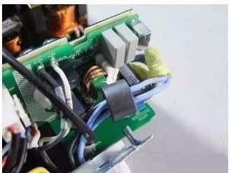
1. First measure the size of the PCB and the number of devices, so that there is a dense, or a dense, a sparse and difficult to see. 2. The circuit is modularized, with the core device as the center, and the principle of priority placement of key devices is to place the device once. 3. The device is set up vertically or horizontally, one is beautiful, the other is convenient for plug-in operation, and special circumstances can be considered tilt. 4. The layout needs to take into account the traces, placed in the most reasonable position to facilitate subsequent traces. 5. The loop area should be reduced as much as possible during the layout, which will be explained after the four major loops. To achieve these points, of course, we must use it flexibly, and a reasonable layout will soon be born. The following is the first virgin PCB board that I painted. Many years ago, it was very difficult to complete. There may be minor problems in the middle, but the general layout is worth studying:
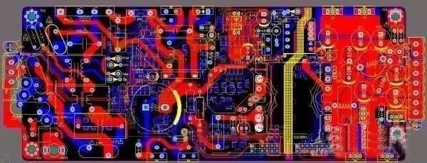
The power density of this figure is still relatively high. The control part of the LLC, the auxiliary source part, and the BUCK circuit driver (high power multiple output) part are not shown on the small board. Let's take a look at the layout characteristics of the main power: 1 The input and output terminals are fixed and cannot be moved. The board is rectangular. How does the main power flow go? Here is used from bottom to top, left and right layout, heat dissipation is dependent on the shell. 2. The EMI circuit is still clear, which is very important. It is also not good for EMC to be uncomfortable. 3. The position of the large capacitor takes into account the PFC loop and LLC main power loop; 4. The secondary side of the current is relatively large, in order to take the current, as well as rectifier cooling, with such a layout, rectifier on the BUCK circuit Under the MOS tube, the heat dispersion effect is good; the high-power top layer generally goes negative, and the bottom layer goes positive. Each board has its own characteristics, of course, has its own difficulties, how to rationally solve is the key, we can understand the rational choice of the meaning of the layout? Seven, PCB instance Appreciation
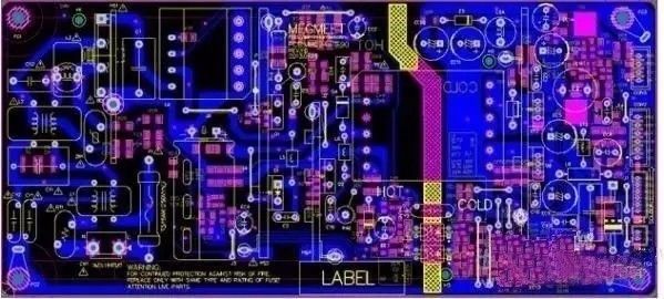
According to the PCB layout points discussed earlier, this board is inspected. Whether it is done is in place. I think it is a good place to do it. Of course, there will always be, and it can be proposed. The single panel is so compact that this can be done. It is not easy, you can use this board to learn and discuss! Behind the board will also explain learning, we first appreciate the next.
Eight, PCB design of the four major loops understanding: (The basic requirement for PCB layout is the small four loop area)
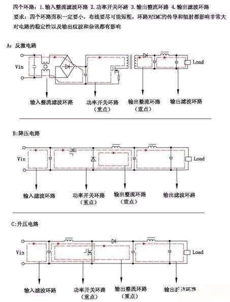
In addition, the absorption loop (RCD absorption and RC absorption of the MOS tube, RC absorption of the rectifier tube) is also very important, and it is also a loop that generates high-frequency radiation. Any questions about the above figure are welcome to discuss and are not afraid of any doubt. As long as it is the question of the problem, discuss learning together to make greater progress! Nine, the hot spot of the PCB design (floating potential point) and ground:
Note: 1. For hot spots, we must pay special attention (high-frequency switching point), is a high-frequency radiation point, layout traces have a great impact on EMC. 2. The loop formed by hotspots is small, the traces are short, and the traces are not as thick as possible, but enough to run the current enough. 3. Ground wire should be grounded at one point. The main power ground is separated from the signal ground, and the sampling ground is left alone. 4. The ground of the radiator needs to be connected to the main power ground. Tenth, EMC rectification experience
Are personal understanding, perhaps with the traditional data materials, there are differences, please consider yourself, anyway, I think a lot of general-purpose teaching results are not my own summary of the use, boasted. There are many things that you may want to say, but it may be a bit chaotic. It is all out of practice! How EMC understands how to generate and test the results of the test: Simply how to prescribe the right medicine, and in many cases get the first round of test results, how will the results and power To contrast analysis; the main ideas are as follows: 1, for the conduction, the test range standard 15K-30M, the common EN55022 is from 150K. How is the source of conduction generated? For low frequencies, mainly the switching frequency and its frequency multiplication (follow-up diagram), this source can not be solved, the switching frequency can not be eliminated, of course, you can change the switching frequency, it is only to move the test results, and There is no real sense of elimination. Can only be solved by the filter, in general for the low frequency using R10K this high flux material has a good effect, the size of the magnetic ring is related to your power, generally reach 10MH sense, even bigger to 20MH, with Y Capacitors are generally well-solved. Low frequencies are not difficult. The real difficulty is high frequencies. Individuals believe that the causes of high frequencies are more complicated. There are switches, transformers, and inductors. This means that everything is on and off. The place may exist (how to determine the specific location, follow-up to explain), there need to be some exploration; find the source may not be able to solve the source, may have improved, or with the filter. For high frequency, using low-flux materials, such as nickel-zinc rings, the sense of inductance is generally UH level, with appropriate Y capacitors (more complex power supply, it is recommended to place more than a few Y capacitor position, facilitate rectification); 2 With some means of cooperation, many textbooks mention increasing the X capacitance to determine the differential mode or the common mode. There is a certain significance that may not be helpful in reality. Generally, we design the X capacitor to a suitable value. And increasing the X-capacitor can solve the problem of differential mode. It is also a matter of fact. Therefore, many textbooks provide guidance in a certain sense. Personally, it feels useless. I think there are several good methods: 1. Comparing the grounding with the incomprehension of summing up the differences, the ungrounded may be even worse because of the less conduction path of the system structure; or there may be improvement, indicating that the ground loop is conducted to the port. . The specific solution is to adjust the point Y capacitance of the circuit ground and add magnetic beads. 2. In the input port ferrule, if the low U ring is improved, adjust the first-stage filter inductance. 3 complex system attention EMI circuit shielding measures. If the measures are not effective, introspect PCB design, this aspect will be mentioned in the PCB design. 3, for radiation: must find the source to solve, observe the first test results, if the 30M near the vicinity, with grounding related to the system to find the ground, and to determine whether the test is well grounded, sometimes the input line has an effect. Within 2.40M-100M, it is generally caused by the opening and closing of the MOS tube. Sometimes it is judged whether it is opened or closed directly for the sake of the site. It can be verified by the targeted rectification observation results. (Of course, this has to spend money. The follow-up will explain how to use Oscilloscope to judge, this is a secret move). 3 More than 100M is caused by a diode, and the diode absorption capacitance is rectified. Some of the high power may be synchronous rectification, and the MOS transistor absorption loop may be changed. Remember that sometimes, when adjusting C, the R must be rectified. Too much to say, follow-up to specific examples to add it, the first to play so much, anyway, I play hard enough, can cause resonance is difficult, after all, everyone's rectification experience is much worse, it should give new friends some inspiration, Follow-up will give an example! Eleventh, the layout of the filter capacitor wiring
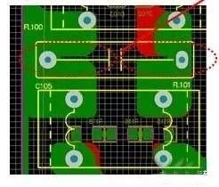
The filter capacitor's trace has a crucial effect on the filtering effect. If it goes bad, it may lose its proper filtering effect. Figure 1 shows the secondary side rectification filtering method to share the effects of the two capacitors and avoid the failure of the second capacitor in the rectification circuit.
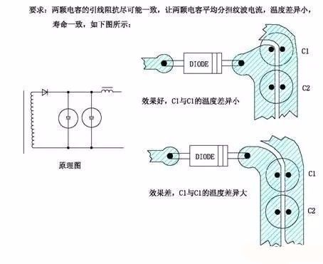
Figure 2: The output filter capacitor wiring, must not be external (that is, bypassed), poor output ripple is poor.
Twelve, LLC circuit layout and EMC
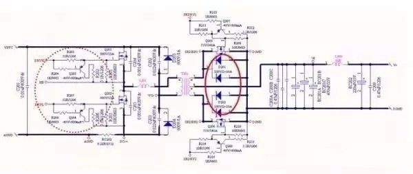
LLC circuit is most familiar to everyone, the dotted circle is the drive circuit, in the design of the circuit close to the MOS tube, which means that the IC driver only needs to pull the two lines to pull the drive circuit, the drive circuit is close to the MOS tube, to avoid Be disturbed (At the same time, we must pay attention to driving the interference to the sensitive signal while routing, both sensitive signal and interference source); once you drive the interfered power, you can imagine. Similarly, the synchronous rectification MOS tube driver should also be close to the synchronous rectifier tube. It can be well understood when designing the schematic diagram as this diagram. If you give this circuit to the PCB engineer layout, he is very intuitive how to layout the traces. If you are drawing a mess, many PCB engineers may have a good understanding of the circuit and may be easily misplaced. In addition: the primary side has an important loop, PFC capacitors and MOS transistors and transformers, resonant inductors, resonant capacitors constitute a small loop area; secondary side rectifier filter loop is equally important, before the capacitance of the cable, it is also very Important; pay attention to the distance between the high and low voltages during the trace. In some places, the voltage is floating and must be treated as a high voltage, such as the upper tube driver and the corresponding reference voltage. As for the EMC aspect, the opening of the LLC is a soft switch. The opening has little impact on EMC. The focus is on the speed of shutting down the speed and impact on EMC. The capacitance of the MOS transistor junction capacitor has a great impact on EMC. The choice of the capacitor is not suitable, or Is not added (MOS tube itself has a junction capacitance) may have an impact on EMC, which is the focus of attention; this figure does not have a Y capacitor, in the MOS tube positive or negative anti-Y capacitor can also be very good to filter out the switching interference; If you have any questions about this circuit, you can discuss it and grow in the discussion! Thirteen, circuit design and layout of the PFC
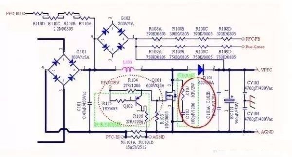
The figure above is a typical BOOST PFC circuit: The green box on the left is the driver circuit. Like the previous LLC topology drive, it is located close to the MOS and is shown on the schematic diagram. The green dashed square box on the right side is the MOS transistor off spike absorption circuit, which is the same as the MOS tube forming the loop; the other two important loops, one is the MOS tube open loop (dotted red figure), and the other is the MOS The tube shuts off the circuit (solid red diagram); loop area is as small as possible; fourteen, magnetic ring in the EMC useless products EMC is difficult to handle at the source, you can use magnetic ring filter, of course, I say here The magnetic ring has two levels of meaning, on the one hand, the input and output filter inductors, using different material magnetic ring, different number of turns will have a corresponding effect, there is also a direct meaning on the input and output lines on the one hand, set the magnetic ring, Sometimes it can be used magically, but it can not be used in all occasions, but at least it can be used as a basis for judgment;
The blue and black lines in the figure above are the positive and negative ends of the output, and a magnetic ring is set on it to solve the high frequency end caused by the output rectifier. In some cases, the interference of the port on the PCB may not be effective. The magnetic ring on the wire has unexpected effects. 15. Key Signals of PCB Traces
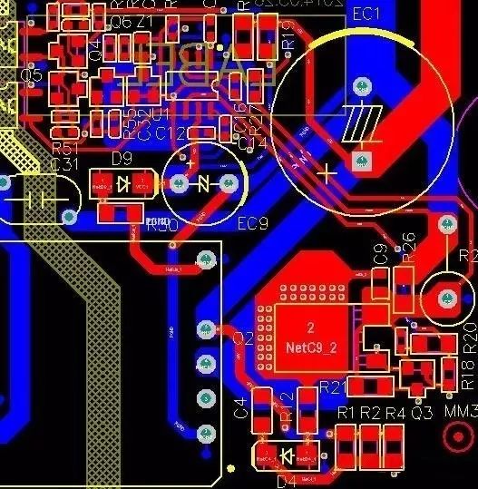
Note: 1. CS signal (sampling signal): Pull out from sampling resistors R25 and R26. Note that the ground of the IC is based on the sampling resistance. The positive and negative differential traces of the sampling resistor pull down the IC CS pin and the GND pin of the IC. 2. The driver signal pulls down the IC driver pin from the driver circuit, taking care not to interfere with the CS pin; as shown in the figure, the three lines are routed side by side, and the ground line will play a certain shielding role in the middle of the driver and the CS line; The panel is best to be shielded by a layer of ground covering of the IC. The network of the ground must be led from the IC GND. The non-key signal GND can be directly punched. The key signal ground needs a single point of grounding, directly connected to the IC; 4.FB feedback network signal Pay attention to the trace and single point access to IC; 5. RCD absorption network should not be placed in the main loop; 6. VCC rectifier filter ground to be connected to the main power ground, secondary filter can be connected to the IC ground; 7.Y capacitor wiring separately , can not be confused with the main power to avoid interference; 16, the main power and control part of the wiring diagram
Many people may see this picture, in the fog, the general introduction: 1. PFC driver and IC common ground PFC tube, more specific point is to connect the sampling resistor; 2. DC-DC part of the drive And control ground to connect the sampled ground of the DC switch part; 3. The auxiliary source part is controlled to connect to the auxiliary source MOS pipe to sample the first, and the MOS pipe to the main power ground again; 4. The power source of the respective IC is filtered through the auxiliary source EC. Ground, pay attention to RC filter close to IC; Summary: pay attention to their own single-point grounding, ground is not chaotic, is one of the most important places to walk! ! ! 17. Analysis of electromagnetic shielding mechanism Figure 1: Principle of magnetic shielding
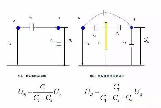
As shown in the figure, the input and output electric field disturbances can be coupled by capacitive transmission. If the shielding plate is added, the size of C4 is increased, and C1 is also reduced, which serves the purpose of attenuation of electric field interference; Figure 2: Principle of magnetic field shielding
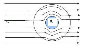
As shown in the figure, the characteristics of magnetic field shielding are different from that of magnetic field. It requires shielding of the housing. The electric field only needs a planar shielding plate. Therefore, the shielding of the radiator brings about electric field shielding, and some cases use the enclosed power supply of the housing to play a certain magnetic field shielding; Principle, the magnetic field through the shield will change the magnetic circuit, resulting in the magnetic flux to the surrounding diffusion, the middle magnetic field interference to achieve the purpose of shielding; 18. Switching devices and EMC understanding of the device is also of great significance to EMC, such as MOS tube, the main switch MOS It is one of the most important sources of EMC, and the turning on and off of the rectifier will also generate high-frequency radiation (the principle is that the magnetic field produces a magnetic field, and the changing current generates an electric field); of course, the semiconductor switching device is mainly introduced here. Other inductors Transformer will not explain; What parameters of the switching device have an important impact on EMC, we often say that fast pipe, what is the reference to slow pipe? We all know that the quick opening of the fast tube is small, and we like to use it for high efficiency. However, for the smooth passage of EMC, we have to abandon the efficiency and reduce the switching speed to weaken the switching radiation. For MOS transistors, the turn-on speed is determined by the drive resistance and the input junction capacitance. Determined; shutdown speed is determined by the output junction capacitance and the internal resistance of the tube;
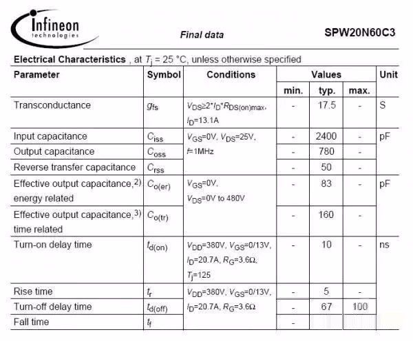
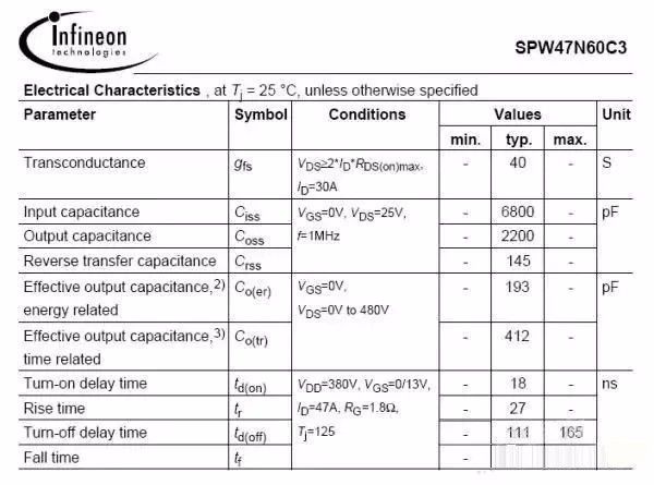
Referring to the above two figures, different types of MOS transistors compare the input junction capacitance and the output junction capacitance, 2400PF and 800PF, 780PF and 2200PF. At first glance, the first specification is the fast tube, and the second is the slow tube. When determining the switching speed must match with the drive resistor; conventional drive resistance in the 10R-150R more, select the drive resistor and junction capacitance related to the fast board drive resistor can be properly increased, slow drive resistance can be reduced; for the diode There are Schottky diodes, fast-response diodes, common diodes, and a relatively small number of SIC diodes. Switching speed SIC diodes are almost zero, which means that there is no reverse recovery, switching radiation is minimal, and losses are minimal. The disadvantage is that it is expensive, so it is rarely used; followed by the Schottky diode, the forward voltage is reduced, the reverse recovery time is short, followed by fast recovery and common diodes; need to compromise between loss and EMC; generally can be taken Change the absorption and set of magnetic beads and other measures to rectify EMC; Nineteenth, EMC filter
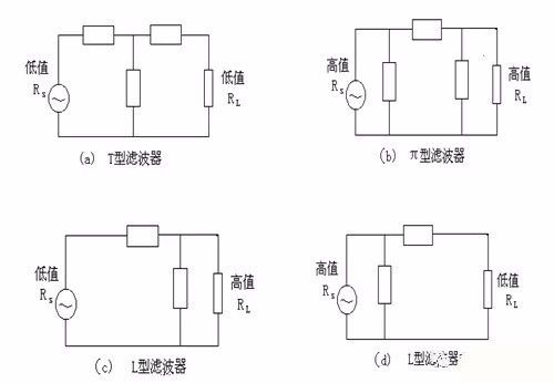
The influence of the filter's architecture choice on the filter is very important. In different occasions, the filter is based on the impedance matching to achieve the filtering effect. Everyone can refer to how to filter according to the principles of this figure; for example, the most commonly used output rectifier bridge is π. Filters and LC filters at the output;
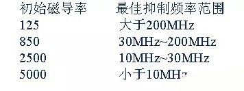
The material of the filter is also crucial for designing the filter inductor. Materials with different initial magnetic permeability will work in different frequency bands. If the wrong material is selected, it will completely lose its effect. 20, EMC's flyback high frequency, etc. Model Analysis
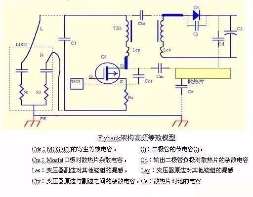
First understand the EMC: EMC path from the simplest model, of course, space radiation is related to the loop, the loop is also constructed by the path; analysis of the high-frequency flyback equivalent model to help understand the mechanism of EMC formation; our test The receiving device will receive the conduction from the L and N terminals. In order to reduce the received interference, the interference must be allowed to circulate through the ground loop without flowing from the L, N port to the receiving device; at this time, our EMI inductance and Y capacitance are matched by impedance matching. Can be achieved; In addition the primary side of the interference can be through the original secondary Y capacitor, transformer stray capacitance and ground coupled to the secondary side, forming more loops; Of course, some of the junction capacitance parameters, such as MOS junction capacitance, heat sink junction capacitance Can form a distribution path; 21, radiation forms and frequency distribution
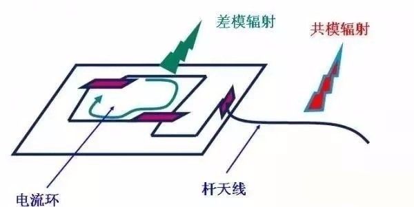
This picture may be somewhat abstract, but it is very difficult for EMC to be specific. We need to give us some inspiration. We can see that: Differential mode radiation is in the form of a loop, and common mode radiation is transmitted in the form of an antenna; As mentioned before, when we lay out the switch loops, we must not use sharp corners during the layout of the switch loops. We usually go at 45 degrees, preferably using arcs. Of course, the wiring efficiency will be relatively low; the basic knowledge of these principles is well understood. It is useful to actually deal with EMC work and layout. If you don't have this awareness, it may be useless, because it can't provide direct methods and needs to combine with other knowledge. And many of the principles mentioned here are in many EMC data. Can not see, but also not so concentrated, you need to experience again!
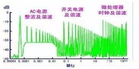
As shown in the figure: The relationship between some frequency terminals and the generating parts of switching power supply, this is only a general rule, do not completely believe that; The law is not established in all cases. The difference between different power sources is also great, so the principle is to help you analyze, not to follow the method; 22, EMC example
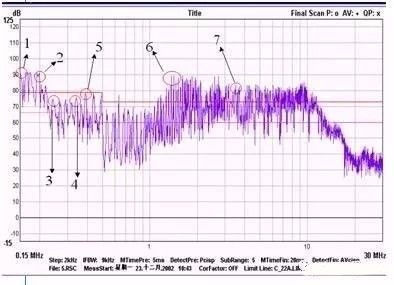
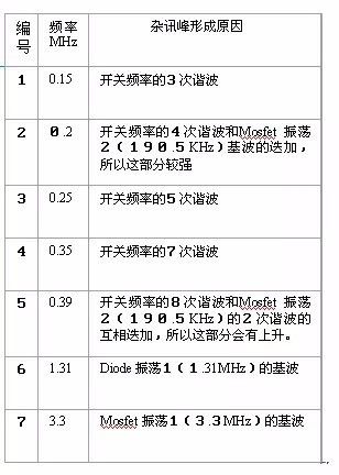
According to the conduction example, the distribution point of the frequency is the relationship between the specific data and the fundamental frequency. After this test, you need to speculate on the laws of these values ​​and you may find clues; of course, how these frequencies are solved by filters. The method was also mentioned in front of it; here is to add to everyone seemingly mysterious EMC how it came from, it feels no longer mysterious, not just a confusing use of filters to solve the problem!
As a mobile multi-purpose platform, tablet computers also provide many possibilities for mobile teaching. The touch-based learning & entertainment teaching platform allows children to efficiently improve their academic performance in a relaxed and pleasant atmosphere. Such tablet computers generally integrate two learning sections of various courses and systematic learning functions. Generally, it includes multi-disciplinary high-quality teaching resources. The education tablet has the following main functions: it has the functions of touch screen input, text editing, picture editing, data storage, data management, wired and wireless Internet access that ordinary tablet computers have; Management functions, search methods support manual search, query by keyword, query by time; text and pictures can be scanned and converted into documents to save.
Education Tablet,learning tablet,leaning machine,New learning tablet
Jingjiang Gisen Technology Co.,Ltd , https://www.jsgisentec.com