Everyone knows that the CPU cache is very important, but little is known about the specific breakdown of the cache. As long as this article is about the introduction of the CPU cache, it focuses on the difference between the first-level cache, the second-level cache, and the third-level cache.
CPU cacheThe CPU cache (Cache Memory) is a temporary storage located between the CPU and the memory. Its capacity is much smaller than that of the memory but the exchange speed is much faster than that of the memory. The appearance of the cache is mainly to solve the contradiction between the CPU operation speed and the memory read and write speed, because the CPU operation speed is much faster than the memory read and write speed, which will make the CPU spend a long time waiting for the data to arrive or write the data RAM. The data in the cache is a small part of the memory, but this small part is about to be accessed by the CPU in a short time. When the CPU calls a large amount of data, it can be called in the cache first to speed up the reading speed.
The capacity of the CPU cache is much smaller than that of the memory, but the exchange speed is much faster than that of the memory. The appearance of the cache is mainly to solve the contradiction between the CPU operation speed and the memory read and write speed, because the CPU operation speed is much faster than the memory read and write speed, which will make the CPU spend a long time waiting for the data to arrive or write the data into the memory .
The size of the cache is one of the important indicators of the CPU, and the structure and size of the cache have a great impact on the speed of the CPU. The operating frequency of the cache in the CPU is extremely high. Generally, it operates at the same frequency as the processor. The work efficiency is much greater than the system memory and hard disk. In actual work, the CPU often needs to read the same data block repeatedly, and the increase of the cache capacity can greatly improve the hit rate of the data read in the CPU, instead of looking for it in the memory or hard disk, thereby improving system performance . But considering the factors of CPU chip area and cost, the cache is very small.
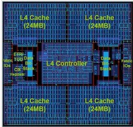
According to the order of data reading and the degree of close integration with the CPU, the CPU cache can be divided into a first-level cache and a second-level cache. Some high-end CPUs also have a third-level cache. All data stored in each level of cache is the next level. As part of the cache, the technical difficulty and manufacturing cost of these three types of caches are relatively decreasing, so their capacity is relatively increasing. When the CPU wants to read a piece of data, it first looks in the first level cache, if it doesn't find it, then it looks up in the second level cache, if it still doesn't, it looks up in the third level cache or memory. Generally speaking, the hit rate of each level of cache is about 80%, which means that 80% of the total data volume can be found in the first level cache, and only 20% of the total data volume needs to be from the second level cache. , Level 3 cache or read in memory, it can be seen that Level 1 cache is the most important part of the entire CPU cache architecture.
What is the difference between the first level cache, the second level cache, and the third level cacheWhat are the first-level cache, the second-level cache, and the third-level cache? effect? the difference? First, let's take a brief look at the first level cache. At present, most mainstream processors have first-level cache and second-level cache, and a few high-end processors also integrate third-level cache. Among them, the first-level cache can be divided into a first-level instruction cache and a first-level data cache. The first-level instruction cache is used to temporarily store and deliver various computing instructions to the CPU; the first-level data cache is used to temporarily store and deliver the data required for operations to the CPU. This is the role of the first-level cache. So, what is the role of the secondary cache? Simply put, the second-level cache is the buffer of the first-level cache: the first-level cache is very expensive to manufacture, so its capacity is limited, and the role of the second-level cache is to store those that are needed for CPU processing and cannot be stored in the first-level cache. data. In the same way, the third-level cache and memory can be regarded as the buffers of the second-level cache. Their capacity increases, but the unit manufacturing cost decreases.
It should be noted that neither the second-level cache, the third-level cache nor the memory can store the original instructions for processor operations. These instructions can only be stored in the first-level instruction cache of the CPU, while the remaining second-level cache and third-level cache And memory is only used to store data required by the CPU. According to different working principles, the current primary data cache used by mainstream processors can be divided into two types: real data read-write cache and data code instruction trace cache, which are used by AMD and Intel respectively. Different primary data cache designs have different requirements for secondary cache capacity. Let us briefly understand the differences between these two primary data cache designs.
1. AMD Level 1 Data Cache Design The level 1 cache design adopted by AMD belongs to the traditional "real data read and write cache" design. The first-level data cache based on this architecture is mainly used to store the first data read by the CPU; and more read data are stored in the second-level cache and system memory respectively. To make a simple assumption, if the processor needs to read the string of data “AMD ATHLON 64 3000+ IS GOOD†(without spaces), then the “AMDATHL†to be read first will be stored in the primary data cache , And the remaining "ON643000+ISGOOD" are stored in the secondary cache and system memory respectively (as shown in the figure below). It should be noted that the above assumption is only an abstract description of the first-level data cache of AMD processors. The length of data that can be stored in the first-level data cache and the second-level cache is completely determined by the size of the cache, and is by no means the above assumption. A few bytes. The advantage of "real data read-write cache" is that data is read directly and quickly, but it also requires a certain capacity of the first-level data cache, which increases the manufacturing difficulty of the processor (the unit manufacturing cost of the first-level data cache is higher than that of the second-level cache ).
2. Intel Level 1 Data Cache Design Since the P4 era, Intel has adopted a new "data code instruction trace cache" design. The first level data cache based on this architecture no longer stores actual data, but the instruction code (that is, the starting address where the data is stored in the second level cache) of the data stored in the second level cache. Assuming that the processor needs to read the string of data "INTEL P4 IS GOOD" (without spaces), then all the data will be stored in the second-level cache, and the first-level data code instruction trace cache needs to store only the above data initial address.
Since the first-level data cache no longer stores actual data, the "data code instruction tracking cache" design can greatly reduce the CPU's requirements for the first-level data cache capacity and reduce the difficulty of processor production. However, the disadvantage of this design is that the data reading efficiency is lower than that of the "real data read-write cache design", and it is very dependent on the capacity of the second-level cache. After understanding the general function and classification of the first level cache and the second level cache, let's answer the following questions raised by the hardware novice netizen.
In theory, the larger the secondary cache, the better the performance of the processor, but this does not mean that doubling the secondary cache capacity can double the performance of the processor. At present, the size of most of the data processed by the CPU is between 0-256KB, the size of a small part of the data is between 256KB-512KB, and only a few data are more than 512KB in size. Therefore, as long as the available primary and secondary cache capacity of the processor reaches 256KB or more, it can cope with normal applications; the secondary cache of 512KB capacity is sufficient to meet the needs of most applications. Among them, for the AMD Athlon 64 and Sempron processors that adopt the "real data read-write cache" design, because they already have 64KB of the first-level instruction cache and 64KB of the first-level data cache, as long as the processor's second-level cache capacity is greater than Equal to 128KB can store enough data and instructions, so they are not very dependent on the secondary cache. This is why Socket 754 Sempron 3000+ (128KB L2 cache), Sempron 3100+ (256KB L2 cache) and Athlon 64 2800+ (512KB L2 cache) with the same 1.8GHz frequency are very close in most evaluations. The main reason. So for ordinary users, 754 Sempron 2600+ is worth considering. On the other hand, Intel’s current P4 and Celeron series processors all adopt the "data code instruction trace cache" architecture. The first level cache of the Prescott core only contains 12KB level one instruction cache and 16KB level one data cache. The Northwood core has only 12KB first-level instruction cache and 8KB first-level data cache.
Therefore, P4 and Celon series processors are very dependent on the secondary cache. The performance gap between Celeron D 320 (256KB secondary cache) and Celeron 2.4GHz (128kb secondary cache) is a good proof; Cayon D and P4E The performance gap between the processors is also very obvious. Finally, if you are an avid game enthusiast or a professional multimedia user, a P4 processor with 1MB L2 cache and an Athon 64 processor with 512Kb/1MB L2 cache are your ideal choice. Because the main memory and secondary cache of the CPU are almost "full" under heavy computing load, the large secondary cache can provide about 5% to 10% performance improvement for the processor, which is absolutely necessary for demanding users of. The first level cache is in the CPU to store internal instructions. The second level cache is packaged with the CPU and is also used to store instruction data. The third and fourth level caches are only available in high-end server CPUs and have similar functions. Faster, more stable, and more effective is not that the larger the cache, the better. For example, AMD and INTER have different theories. AMD believes that the larger the first-level cache, the better, so the first-level is larger, while INTER believes that the larger the cache is, the longer it is. Instruction execution time, so the first level is very small, and the two companies’ theories of the second level cache are reversed. AMD’s is small and INTER’s is large. Generally, the level 2 cache of mainstream INTERCPU is around 2M. We usually use (L1, L2) to call the cache, also known as the high-speed buffer memory, its function is to alleviate the contradiction between the slow speed of the main memory and the inability to keep up with the CPU read and write speed. Its implementation principle is to copy the small amount of information (data or instructions) that the CPU is most likely to use recently from the main memory to the CACHE. When the CPU uses this information next time, it does not need to access the slow main memory. Obtained directly from the fast CACHE, thereby improving the speed of obtaining these information, so that the CPU has a higher operating efficiency.
Cache size
Generally speaking, a larger cache capacity is good for improving the hit rate. As shown in Figure 4.20, because the cache is implemented with a very expensive static memory SRAM device, and after the cache capacity reaches a certain size, Increasing its capacity will not significantly improve the hit rate. Considering a reasonable performance/price ratio, the cache capacity should be set within a reasonable capacity range. The cache should be divided into one level, two level and three level, in order to establish a hierarchical storage structure to achieve the highest cost performance. Moreover, the multi-level organization can also increase the hit rate of the cache and improve the execution efficiency.
The CPU cache (Cache Memory) is a temporary storage located between the CPU and the memory. Its capacity is much smaller than that of the memory but the exchange speed is much faster than that of the memory. The appearance of the cache is mainly to solve the contradiction between the CPU operation speed and the memory read and write speed, because the CPU operation speed is much faster than the memory read and write speed, which will make the CPU spend a long time waiting for the data to arrive or write the data into the memory . The data in the cache is a small part of the memory, but this small part is about to be accessed by the CPU in a short time. When the CPU calls a large amount of data, it can avoid the memory and call it directly from the cache, thereby speeding up the reading speed. . It can be seen that adding a cache to the CPU is an efficient solution, so that the entire internal memory (cache + memory) becomes a storage system with both the high speed of the cache and the large capacity of the memory. The cache has a great impact on the performance of the CPU, mainly due to the CPU's data exchange sequence and the bandwidth between the CPU and the cache. The working principle of the cache is that when the CPU wants to read a piece of data, it first looks it up in the cache, if it finds it, it reads it immediately and sends it to the CPU for processing; if it doesn’t find it, it reads it from the memory and sends it to it at a relatively slow speed. CPU processing, and at the same time transfer the data block where this data is located into the cache, so that the entire block of data can be read from the cache in the future, without having to call the memory. It is this read mechanism that makes the CPU read cache hit rate very high (most CPUs can reach about 90%), which means that 90% of the data that the CPU will read next time are in the cache, only about 10% Need to read from memory.
This greatly saves the time for the CPU to directly read the memory, and also makes the CPU basically no need to wait when reading data. In general, the order in which the CPU reads data is cached first and then memory. At present, the cache basically uses SRAM memory. SRAM is the abbreviation of English Static RAM. It is a memory with static memory access function. It can save the data stored in it without refreshing the circuit. Unlike DRAM memory, which requires a refresh circuit, the DRAM must be refreshed and charged every once in a while, otherwise the internal data will disappear, so SRAM has higher performance, but SRAM also has its shortcomings, that is, its integration. Lower, the same capacity of DRAM memory can be designed into a smaller volume, but SRAM needs a large volume, which is also an important reason why the cache capacity cannot be made too large at present.
Its characteristics are summarized as follows: the advantages are energy saving, fast speed, no need to cooperate with the memory refresh circuit, which can improve the overall work efficiency, but the disadvantages are low integration, large volume of the same capacity, and high price, which can only be used in a small amount for the key. Sexual system to improve efficiency. According to the order of data reading and the degree of close integration with the CPU, the CPU cache can be divided into a first-level cache and a second-level cache. Some high-end CPUs also have a third-level cache. All data stored in each level of cache is the next level. As part of the cache, the technical difficulty and manufacturing cost of these three types of caches are relatively decreasing, so their capacity is relatively increasing. When the CPU wants to read a piece of data, it first looks in the first level cache, if it doesn't find it, then it looks up in the second level cache, if it still doesn't, it looks up in the third level cache or memory. Generally speaking, the hit rate of each level of cache is about 80%, which means that 80% of the total data volume can be found in the first level cache, and only 20% of the total data volume needs to be from the second level cache. , Level 3 cache or read in memory, it can be seen that Level 1 cache is the most important part of the entire CPU cache architecture.
Level 1 Cache (Level 1 Cache) is abbreviated as L1 Cache. It is located next to the CPU core and is the most closely integrated CPU cache. It is also the earliest CPU cache in history. Because the technical difficulty and manufacturing cost of the first-level cache are the highest, the increased technical difficulty and cost increase brought about by increasing the capacity are very large, but the performance improvement brought by it is not obvious, the cost performance is very low, and the existing first-level cache hits The rate is already very high, so the first level cache is the smallest of all caches, much smaller than the second level cache. Generally speaking, the first-level cache can be divided into the first-level data cache (Data Cache, D-Cache) and the first-level instruction cache (InstrucTIon Cache, I-Cache). The two are used to store data and decode the instructions that execute these data in real time, and both can be accessed by the CPU at the same time, reducing conflicts caused by contention for Cache, and improving processor performance. At present, the first level data cache and the first level instruction cache of most CPUs have the same capacity. For example, AMD’s Athlon XP has a 64KB level one data cache and a 64KB level one instruction cache. The first level cache is 64KB+64KB. Indicates that the representation method of the first level cache of the rest of the CPU is analogized.
Intel's CPU with NetBurst architecture (the most typical is PenTIum 4) has a special level of cache. It uses a newly added level 1 trace cache (ExecuTIon Trace Cache, T-Cache or ETC) to replace the level 1 instruction cache. , The capacity is 12KμOps, which means that it can store 12K, that is, 12000 decoded microinstructions. The operating mechanism of the first-level tracking cache and the first-level instruction cache is different. The first-level instruction cache only decodes instructions in real time without storing these instructions, and the first-level tracking cache also decodes some instructions. Instructions are called micro-ops, and these micro-instructions can be stored in the first-level trace cache, and there is no need to decode the program every time. Therefore, the first-level trace cache can effectively increase the number of instructions under high operating frequency. The decoding ability of the micro-ops, and μOps is micro-ops, which means micro-operation. It provides μops to the processor core at a very high speed. The Intel NetBurst micro-architecture uses an execution tracking cache to separate the decoder from the execution loop.
This trace cache provides uops to the core with a high bandwidth, which is essentially suitable for making full use of the instruction-level parallel mechanism in the software. Intel has not announced the actual capacity of the first-level tracking cache. It only knows that the first-level tracking cache can store 12,000 micro-ops (micro-ops). Therefore, we cannot simply use the number of microinstructions to compare the size of the instruction cache. In fact, the single-core NetBurst architecture CPU using 8Kμops cache is basically enough, and the extra 4kμops can greatly improve the cache hit rate. And if you want to use hyper-threading technology, 12KμOps will be somewhat insufficient, which is why sometimes Intel processors will cause performance degradation when using hyper-threading technology.
For example, the Northwood core's first-level cache is 8KB+12KμOps, which means its first-level data cache is 8KB, and the first-level tracking cache is 12KμOps; and the Prescott core's first-level cache is 16KB+12KμOps, which means its first-level data cache is 16KB , The first-level tracking cache is 12KμOps. Here, 12KμOps is definitely not equal to 12KB, and the units are all different, one is μOps and the other is Byte (byte), and their operating mechanisms are completely different. So those who simply add up the first level cache of Intel's CPU, for example, say that the Northwood core is a 20KB first-level cache, and the Prescott core is said to be a 28KB first-level cache, and based on this, think that the first-level cache capacity of Intel processors is far The view that the primary cache capacity of AMD processors is lower than 128KB is completely wrong, and the two are not comparable. In the comparison of CPUs with different architectures, it is difficult for many caches to find the corresponding things. Even caches with similar names have different design ideas and function definitions. At this time, simple arithmetic addition cannot be used for comparison; and in the architecture In a very similar CPU comparison, it makes sense to compare the cache sizes of various functions separately.
ConclusionThat's it for the breakdown of caching. I hope this article will help you.
80 Plus Gold
Boluo Xurong Electronics Co., Ltd. , https://www.greenleaf-pc.com