IntroductionVarious electric and electromagnetic disturbances generated inside and outside a car can be hazardous to vehicle electronic equipment. They can degrade performance, cause malfunctions, and even destroy electronic devices. The most severe disturbances—large positive and negative overvoltages and transients—can be generated in the vehicle's electrical system itself or be applied to it from external sources due to (erroneous) human interaction.
Transient Voltages Generated Inside the CarIn an automotive network, electronic control units (ECUs) are interconnected through the wiring harness. Most ECUs are powered by the car battery, either directly or through the ignition switch. Even during normal operation, electrical disturbances and high- frequency effects can occur, and be distributed across the wiring harness to the onboard electronics by conduction and capacitive or inductive coupling. Sources of disturbance include the ignition system, the alternator, load switching, switch bounce, and "load-dump" effects, ie , voltages generated by DC motors that are disconnected from their supply while running.
The most aggressive of these surges is the so-called "load-dump pulse" (Figure 1). This transient occurs when the engine is running and the battery lead is disconnected, due to a poor connection or accidentally while the alternator is charging the battery. The magnitude of that transient depends on the alternator's rotational speed and field excitation at the moment of disconnection. The surge can last several hundred milliseconds and reach levels of over 100V, which is potentially lethal to semiconductor circuits.
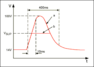
Figure 1. Typical load-dump surge shape: a) unsuppressed; b) suppressed.
Jump Start, Cold Crank, and Battery ReversalAnother danger is the "double battery" voltage that can be applied during a jump start, ie, when hooking up with jumper cables to another vehicle's battery with a 24V network system, so that you end up using a 24V battery to start a 12V system. Consider the following situation: you crank the engine, especially in cold weather and with a partly charged battery, and the engine oil has become very thick. The engine cranking requires the starter to deliver more torque, which, in turn, needs more current from the battery. This large current load causes a brief "dip" in supply voltage, a dip that can depress the voltage from a nominal 12V to less than 5V. This reduction can last for several tens of milliseconds, causing electronic systems to temporarily suspend operation (Figure 2). Once the engine starts, the voltage returns to its nominal value.
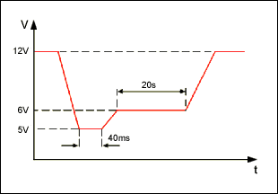
Figure 2. Typical vehicle cold crank voltage shape.
An additional hazard that vehicle electronics must withstand is battery-polarity reversal, which can occur when a battery is incorrectly attached to the electrical system (eg, -14V).
Protection Against Improper Power LevelsThe disturbances mentioned above create a need for protection against improper voltages. Analysis shows that the load-dump pulse is the most energy-rich type of disturbance. To protect electronic modules against destruction by this pulse, two protection methodologies are used today: Clamp the voltage centrally for all modules at the vehicle alternator (central load-dump suppression, Figure 1b). Provide a protection circuit on each ECU. Secondary suppression, however, is still required to protect against other, locally generated, lower- energy pulses like short positive and negative transients and battery reversals. Those pulses are usually filtered at the board level only by small and high-value capacitors, reverse-polarity diodes, or series inductances augmented by a transient-voltage-suppressor (TVS) diode or varistor.
Centralized load-dump suppression is usually achieved by clamping circuitry (diodes) internal to the alternator. This approach is designed to absorb load-dump energy and to withstand full jump-start voltage. Therefore, the clamping voltage is set higher than the maximum jump -start voltage that can occur. In this case, the vehicle voltage can still reach as high as 36V.
Vehicle electrical systems that do not feature central load-dump suppression must include local protection against that load-dump pulse. Local protection is usually done with a protection circuit internal to the ECU, just beyond the connector terminals. Such protection is needed at many locations within the car and, therefore, requires a large number of components with consequent effects on the total leakage current and overall cost. Onboard load-dump protection is usually achieved with TVS diodes (similar to zener diodes), varistors, and suppression filters which should be connected to the power terminals.
Various sample circuits showing classical on-board protection are shown below.
Standard Overvoltage-Suppression DevicesSeveral devices can clamp overvoltages at the board level.
TVS DiodesAvalanche diodes (very similar to zener diodes, Figure 3) are used as clamping devices to suppress all overvoltages above their breakdown voltage. Their especially high energy-absorption capability protects electronic circuits against overvoltage spikes and load dump. These diodes feature very fast switch -on times, but slow switch-off times. An avalanche diode can respond to overvoltages faster than other common overvoltage-protection components such as varistors. Their performance does not degrade with lifetime and the number of applied transients. When approaching their breakdown voltage, avalanche suppression diodes exhibit significant leakage current. Often these diodes are referred to as Transil®, TransZorb®, or simply TVS diodes.
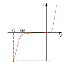
Figure 3. Transient voltage suppressor characteristic (VBR = breakdown voltage, VC = clamping voltage @ peak pulse current, IP).
Varistors Varistors are voltage-dependent resistors (VDRs). They are symmetrical, nonlinear resistive elements whose resistance decreases abruptly above a certain voltage (Figure 4). In clamping both positive and negative voltages, their behavior is similar to two back-to-back zener diodes. They handle high levels of current and energy for their small size and cost, but they exhibit relatively high leakage current as the applied voltage approaches the clamping voltage. The clamping voltage also increases significantly with applied current. Varistors degrade from repeated exposure to surges , and generally have a higher "clamping voltage" and a significantly slower reaction time compared to TVS diodes.
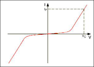
Figure 4. Typical varistor characteristic (VC = clamping voltage @ peak pulse current, IP).
Discrete Protection CircuitsA simple and cost-effective way to protect sensitive circuitry is to parallel the load with a clamp such as a TVS diode and a capacitor preceded by a fuse (Figure 5). This circuit protects the ECU against transient overvoltages and load-dump voltages above the breakdown voltage of the TVS diode (D1). When exposed to high-energy negative transients or steady-state reverse voltages, the TVS is biased in the forward direction, thus protecting downstream circuitry by limiting the negative voltage to its forward bias voltage (eg, -1V). Repetitive low-energy negative transients, such as induced by relay or solenoid switching, are filtered by the capacitor (ClowE). If either negative or positive overvoltages persist, the fuse will blow.
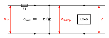
Figure 5. A simple overvoltage protection circuit using a filter capacitor, transient suppressor diode, and fuse.
To avoid having to replace a fuse in the vehicle's fuse box or in an inaccessible ECU, and to ensure continuous ECU operation, other techniques must be employed, such as additional series protection. The circuit of Figure 6 protects the ECU against reverse-battery conditions and transient negative voltages (D2) and impulse positive overvoltages (load dump and low energy transients) greater than the breakdown voltage of the TVS diode (D1). Note that for D2 you must choose a peak reverse voltage greater than the largest possible negative transient .
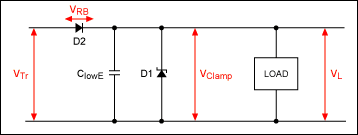
Figure 6. By replacing the fuse used in Figure 5 with a diode, this circuit provides overvoltage protection. It also protects against negative transients and reverse battery connections.
Because of their small dimensions, low cost, and high energy-absorption capability, varistors are often chosen for applications in which board space is critical and the downstream circuitry has some tolerance for positive and negative overvoltages. The circuit of Figure 7 protects the downstream circuitry from overvoltage pulses (positive and negative transients) greater than the breakdown voltage of the varistor. The capacitor helps filter low-energy positive and negative transients.
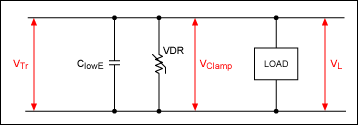
Figure 7. When board space is limited, a varistor (in this case, a VDR) can be used instead of a TVS diode when you want to protect the downstream circuitry from overvoltage pulses (positive and negative transients) greater than the breakdown voltage of the varistor. In this case, the downstream circuits must have some tolerance for positive and negative overvoltage occurrences.
Advantages and Disadvantages of Discrete Protection CircuitsAll of the above circuits have advantages and disadvantages. Figure 5 shows a simple transient protector circuit, consisting only of a TVS, a filter capacitor, and a fuse. However this circuit has several drawbacks. The TVS diode must have a breakdown voltage greater than the highest steady-state voltage present, which is usually the double-battery voltage applied during jump start (often> 26V, for greater than 1 minute). If the wrong TVS diode is used, the TVS starts conducting at a lower-level voltage and is destroyed by the resulting power.
Since the VI characteristics have a predefined slope above the breakdown voltage, TVS diodes exhibit a certain internal resistance, which causes the clamping voltage to increase significantly at high currents. For example, a 28V TVS diode (such as the SMBJ28) can allow the downstream circuitry to be exposed to as much as 45V during a load dump. Exposure to that much voltage thus mandates the use of downstream circuitry tolerant to 45V (Figure 3). Clearly, this requirement complicates the selection of components for downstream ECU circuits, which need to operate only to the upper end of the vehicle's normal operating voltage range (usually about 17V). Finally, higher-voltage semiconductors and other devices are bigger and more expensive, add cost to the ECU and consume valuable board space.
To keep the maximum possible overvoltage as low as possible, a TVS with breakdown voltage as close to the highest possible steady-state voltage (the jump-start voltage, for example) should be used. This choice, in turn, impacts the leakage current at voltages close to the breakdown voltage, and even at the vehicle's normal operating voltage (12V). Such leakage current can make it more difficult for the ECU designer to meet the OEM's (original equipment manufacturer's) requirements for low quiescent current when the vehicle engine is not running.
During normal operation, the diode in Figure 6 (D2) exhibits a voltage drop> 0.7V, which is a disadvantage in two ways: The voltage drop implies some power dissipation. Low-voltage operation of the ECU becomes more difficult. For high- current applications such as a car's antilock braking system, the current drawn can easily exceed 10A. For example, a diode voltage drop of 1V in this system consumes 10W, which is almost impossible to dissipate over the limited geometry of a circuit board. The use of a single or double Schottky diode can alleviate this problem in some applications. Assuming a voltage drop of 0.5V, the power dissipation of a double Schottky diode would be 5W at a 10A load current. This value is still high, however, and may oblige the designer to use a big heatsink.
As mentioned above, the voltage loss of a diode drop can itself be a problem. In a 14.4V audio system, for example, you maximize the output power by maximizing the voltage available for driving the speaker. Thus, a loss of 1V in the power supply due to the reverse-battery diode corresponds to an output-power loss of approximately 8.4dBW (for a 2Ω bridge-tied speaker).
When an ECU must operate down to the low-voltage levels that occur while cranking a vehicle at cold ambient temperatures (Figure 2), the loss of any voltage can be critical. During a cold crank, input voltages of 5.5V and lower are common in car manufacturer specifications. The forward voltage drop of a reverse-battery diode can consume precious headroom. If, for example, the car battery voltage drops to 5.5V at the ECU input connector, minus a 0.7V diode drop for the reverse-battery diode, the remaining voltage for the rest of the circuitry is only 4.8V.
If a 5V microcontroller is supplied by a linear regulator with dropout voltage of 500mV, then the microcontroller receives only 4.3V, which might not be sufficient to keep it operating. The microcontroller could go into reset, lose its memory, or cause the whole ECU to temporarily suspend operations. One illustration of this problem can be seen with a GPS navigation system—if you enter the coordinates of the destination before starting the car, it is imperative that data not be lost during a subsequent cold crank.
For applications that include varistors, as in Figure 7, the circuit-board space is often critical. As with TVS diodes, the varistor clamping voltage must be selected according to the highest steady-state DC voltage present. However, the VI characteristic of a varistor above its breakdown voltage rises much more slowly than that of a TVS diode (Figure 4). For that reason, a varistor passes on much higher voltages to the subsequent circuitry than does a TVS diode. The downstream circuitry should be designed accordingly, which could necessitate an increase in the component cost, package dimensions, and board space consumption.
Minimizing overvoltage by setting the clamping voltage to relatively low levels worsens the quiescent current drawn in normal operating conditions. Quiescent current at the normal operating voltage is generally higher than that of a comparable TVS diode, but that effect depends on the component chosen.
Active Transient-Protection AlternativeGiven the aforementioned drawbacks of discrete protection circuits, active protection might be a good alternative. For applications that require low quiescent current, low-voltage operation, reverse-battery and overvoltage protection, and high efficiency, then overvoltage protection circuits such as the MAX16013 / MAX16014¹ are good choices.
The operating principle for these devices is quite simple (Figure 8). These ICs monitor input voltages on the supply rail, and isolate the load from the fault by controlling two external pFET pass switches. The external MOSFETs are turned on between 5.5V and the set upper rail, adjustable by a resistor-divider on the SET pin to a value (usually) between 20V and 28V.
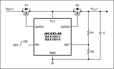
Figure 8. The MAX16013 and MAX16014 provide active transient protection by monitoring the input voltages on the supply rail. When they detect a fault, they isolate the load from the fault by controlling two external p-channel FET pass switches.
During fault conditions the FET P2 can behave in two different ways. In the first mode, P2 is simply a switch that turns off for as long as the overvoltage condition persists, thereby preventing high voltages from damaging any downstream devices. In the second mode, P2 acts as an adjustable transient suppressor that regulates the output voltage to the maximum overvoltage allowed.
When the output voltage rises above the adjusted overvoltage threshold, an internal comparator pulls GATE2 to VCC. When the monitored voltage goes below the overvoltage threshold, the p-channel MOSFET (P2) is turned on again. This process continues to keep the voltage at the output regulated to within approximately a 5% window. The output voltage is regulated during the overvoltage transients; the MOSFET (P2) continues to conduct during the overvoltage event, operating in switched-linear mode and thereby allowing continuous operation while providing overvoltage protection.
The operating mode is selected by connecting the resistor-divider on the SET pin either to the input or to the output. For example, the MAX16013 is configured as an overvoltage switch-off device by connecting the resistive divider to VCC instead of the load. The MAX16014, however, keeps the MOSFET (P2) latched off until the input power is cycled or EN is toggled. Operating the MAX16013 in voltage-limiter mode for long durations elevates power dissipation in the external MOSFETs, due to the voltage drop across them .
The reverse-battery FET (P1, optional) in Figure 8 replaces the series diode suggested in Figure 6. In Figure 8, P1 turns on under forward-bias conditions to minimize the forward voltage drop; it turns off at negative voltages. The EN pin provides shutdown control by turning off P2 and disconnecting the input from the output (Figures 8 and 9). (Note: The signal to the EN pin can be generated by other monitoring circuits in the host system.) Thus, quiescent current in the downstream circuitry is reduced to a minimum (<20µA typical), while the circuit maintains reverse-battery protection (P1).
Active High-Voltage Transient Protectors Offer Advantages over the Conventional Approach Active overvoltage protectors offer several advantages.
As noted above, a discrete transient suppressor (TVS diode or varistor) should have a breakdown voltage higher than the highest steady-state voltage in the vehicle (usually about 26V). During a load-dump event, the downstream circuitry temporarily sees a much higher voltage (an estimate is 45V) due to the internal resistance and VI rising characteristics of the TVS. One must, therefore, select downstream devices capable of tolerating higher voltages. In contrast to that traditional approach, an active transient protector limits output voltage to the level set by the resistor-divider (eg, 26V), and has no rising characteristic. These features let you use lower cost (lower voltage) downstream components.
In contrast to ordinary surge suppressors, which can handle just a few joules for short periods before overheating, the solution based on the MAX16013 / MAX16014 protects against DC overvoltage. Some applications need operate only to the upper end of the normal operating-voltage range, and then switch off. (An audio system, for instance, might operate only up to 17V.) Using an active protector in this case and setting the threshold of the voltage limiter / switch to this level, can reduce the downstream parts cost even more .
Replacing a standard reverse-battery diode with a FET can reduce the voltage drop in forward bias to millivolt levels. Especially in high-current applications, this substitution can reduce power dissipation, which in turn reduces the cooling effort and saves cost. Moreover, the power (voltage), which would otherwise be lost in a diode, is delivered to the load (eg, a speaker). Enhanced output power (performance) can be achieved in this way. Some applications must operate at low battery voltages (when cold cranking an automobile, for instance) and still maintain reverse-battery protection. Minimizing the voltage drop with an active protector can be essential in keeping circuitry operating at low input voltages.
Varistors tend to exhibit relatively high quiescent or leakage current and their lifetime and accuracy significantly degrade due to pulse exposure. Replacing a varistor with an active protector obviates that problem. Some applications have high quiescent current due to leakage currents in devices connected to the battery rail . In those cases, an active protector can serve as a main switch that disconnects (by the P2 FET) all subsequent loads in sleep mode (Figure 9).
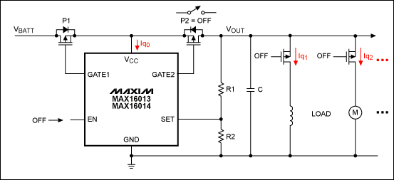
Figure 9. The MAX16013 / MAX16014 are used as the main switch to reduce quiescent current consumption if an ECU is in OFF mode.
SummaryThe use of active overvoltage protectors can be an advantage in some applications. These devices offer significant benefits in reduced power dissipation, output power gain (performance), low-voltage operation (cold crank), lower quiescent current, and lower cost for the downstream circuitry.
¹Related parts: MAX6397 / MAX6398 / MAX6399, MAX6495–MAX6499.
A similar article was published the February, 2008 edition of Auto Electronics Magazine, a Penton Publication.
Transil is a registered trademark of ST Microelectronics.
TransZorb is a registered trademark of Vishay Intertechnology, Inc.
Clients to use iseeled's digital RGB led pixels for the stage led case. If you have any similar projects, welcome to use our digital RGB led pixels. Iseeled's Dmx Led Pixel Light is the high quality and professional led lighting, it is a good choice. Our pixel lights have the 30mm point light, 50mm point light, 100mm point light, 120mm point light for your digital RGB led pixels project. What's more, we don't only offer the pixel lights, but also offer the corresponding Artnet Controller for you. If you have your own controller for the Led Pixel Lights, it's okay. As long as, they are the standard DMX512 controller.
Photo show of DMX LED Pixel Light:


DMX LED Pixel Light
Dmx Led Pixel Light,Digital Rgb Led Pixel Light,Stage Led Pixel Light
Shenzhen Iseeled Technology Co., Ltd. , https://www.iseeledlight.com