Here are some typical processing procedures of digital TV.
Figure 07-04-9 is a block diagram of digital processing in the studio. The signal source sends R, G, and B signals to the color camera, which are converted into digital video signals by A / D and sent to the program production unit. At the same time, the signals from the digital video recorder, digital special effects, and digital system converter are all sent In the program production unit, the signal after the production of the program is sent to the D / A converter to become an analog signal, and then sent to the TV transmitter.
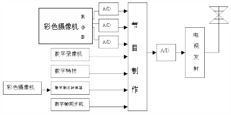
Figure 07-04-9 Studio digital processing block diagram
Figure 07-04-10 is a block diagram of a digital TV transmission system. The originator produces color TV images from the camera. After A / D conversion, it becomes a digital video signal and is sent to the source code. The source code undertakes the compression function of the image data, it removes the redundant part in the signal, and reduces the transmission code rate. The image signal encoded by the source is sent to the multiplexer for multiplexing with the digital audio signal, and then sent to the channel encoder. The channel coding is error correction coding, which improves the anti-interference ability of the signal during transmission. . This is because the data code stream inevitably introduces noise after long-distance transmission and bit errors occur. Therefore, an error correction code is added to improve its anti-interference ability. The signal after error correction coding is sent to the output interface circuit. The output interface circuit plays a role of code type conversion, that is, the unipolar code is changed into a bipolar code which is favorable for transmission. For long-distance transmission, digital microwave lines or digital optical fiber lines can be used, and the distance between stations can reach 50 kilometers by relay transmission. The process of the receiving end is opposite to the sending end. After the receiving end receives the signal, the input interface circuit converts the bipolar signal into a unipolar signal, and then sends it to the channel decoding. In the channel decoding, the error code caused by transmission can be corrected, The signal is sent to demultiplexing, and then sent to the video and audio processing circuits, respectively, and restored to analog video and audio signals.
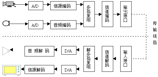
Figure 07-04-10 Block diagram of digital TV transmission system
The block diagram of the digital TV receiver is shown in Figure 07-04-11. The signal received by the TV receiving antenna is amplified by the high frequency channel and the intermediate frequency, and then sent to the video detection to obtain the analog signal. After A / D conversion, it becomes a digital signal, which is sent to a digital processor for digital noise reduction, digital contour correction, digital de-ghosting, line frequency doubling, de-flicker processing, picture-in-picture processing, etc., and finally sent In the D / A converter, it becomes an analog signal for display by the picture tube. The high-frequency part of the TV transmitter and the high-frequency channel part of the TV receiver are both analog systems. This is because it is impossible to achieve digitalization at a frequency close to 1000 MHz at the current technical level.
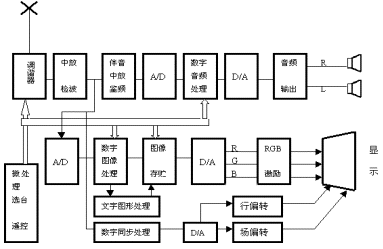
Figure 07-04-11 Block diagram of digital TV receiver
Encoding digital TV signals can be divided into full signal encoding and component encoding, as shown in Figure 07-04-12. Figure (a) is full signal coding, and Figure (b) is component signal coding. It can be seen from the figure (a) that the analog full TV signal is converted into a digital signal by A / D conversion, and after digital processing, it is sent to the D / A conversion to restore the analog full signal. The full signal encoding seems simple from the block diagram, but this method is easy to cause bright and color interference. Especially for the SECAM system (color TV system in Eastern European countries), since the modulation method of the sub-carrier frequency by the color-difference signal is frequency modulation, it is difficult to use full-signal encoding and only component encoding. Figure (b) is a block diagram of component signal encoding. After the analog full signal is A / D converted, it is then digitally bright and color separated, divided into a digital brightness signal and a digital color difference signal, and sent to a digital signal processor. The processed signal Then it is coded by digital full signal, and then it becomes analog full signal by D / A. Although the figure adds digital bright, color separation and digital full-signal encoding, digital processing is performed on the component signals, eliminating the phenomenon of bright and color interference. This processing method can improve the image quality, so it is widely used, and international standards also recommend the use of component signal encoding.
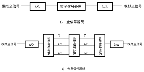
Figure 07-04-12 Full signal encoding and component encoding
Specification:
1. Current:10A,Voltage:125V
2. Material: 100% pure new PC, brass terminal w
3. Certification:UL&CUL.
4. Different colors as customized.
5. OEM service offered here
Product application:
â– Products for commercial,household,lighting
Product features:
â– Good contact
--The contact point composite silver layer is designed to reduce
the contact resistance and reduce the temperature rise.
â– Ultra high strength,impact resistance and thermal stability
--The upper cover is made of high quality polycarbonate and the
bottom shell is made of PA6
â– Chemical corrosion resistance
-- Fingerprint-resistant zinc plated mounting brackets
â– Grounding
--One-piece grounding desig
Gang Switch UL,Wall Gang Switch UL,Electrical Gang Switch UL,Electrical Push Gang Switch UL
Hoojet Electric Appliance Co.,Ltd , https://www.hoojetgfci.com