PIN diodes are commonly used as variable attenuators for RF signals in TV tuners and broadband RF in fixed communication equipment. This type of diode can be mounted on a circuit board as a discrete device or integrated into a hybrid GaAs module. In the high frequency band, the forward resistance of the PIN diode decreases as the junction current increases (Figure 1).
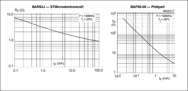
Figure 1. Typical PIN diode resistance vs. forward current
PIN diode attenuators can be used in series or parallel configuration. Series attenuators (Figure 2a) usually require a diode current of 10mA to 20mA. The attenuation is:
20log (1 + RPIN / 2Z0)
 (In dB)
 For parallel attenuators (Figure 2b), the required bias current is usually 2mA to 3mA. The attenuation of the parallel attenuator is:
20log (1 + Z0 / 2RPIN)
(In dB) 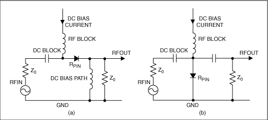
Figure 2. RF signal attenuation by PIN diodes configured in series (a) or parallel (b)
The system controller can change the attenuation by adjusting the diode current.
Some systems may require temperature compensation (Figure 3). In a simplified circuit, the digital potentiometer IC establishes a fixed or adjustable bias level, and the thermistor provides temperature input. These two inputs are connected to an operational amplifier, and the resulting output drives the PIN diode through a resistor.
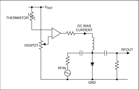
Figure 3. PIN diode simplifies the bias circuit
The implementation of the above circuit is not as simple as the circuit diagram. The response of the thermistor must match that of the PIN diode. At the same time, the change of the bias current will change the forward DC voltage of the PIN diode, which will cause the nonlinearity of the bias current. You can also use a voltage output DAC to replace the thermistor and digital potentiometer to digitally compensate the circuit, but this method cannot eliminate the effect of the forward voltage of the diode. A more ideal method is to use a current source DAC (for ideal solutions, refer to the appendix).
The circuit of Figure 4 also includes a quadrature matched parallel attenuator and a pair of matched PIN diodes driven by the DAC output. The ambient temperature is measured by an analog or digital sensor connected to the host microcontroller, where the host microcontroller performs temperature compensation through a look-up table (LUT) or algorithm. The desired attenuation is set by the LUT or algorithm to the DAC, giving the required PIN current. The current of the PIN diode is set only by the DAC, regardless of the forward voltage of the diode and any other DC impedance in the line.
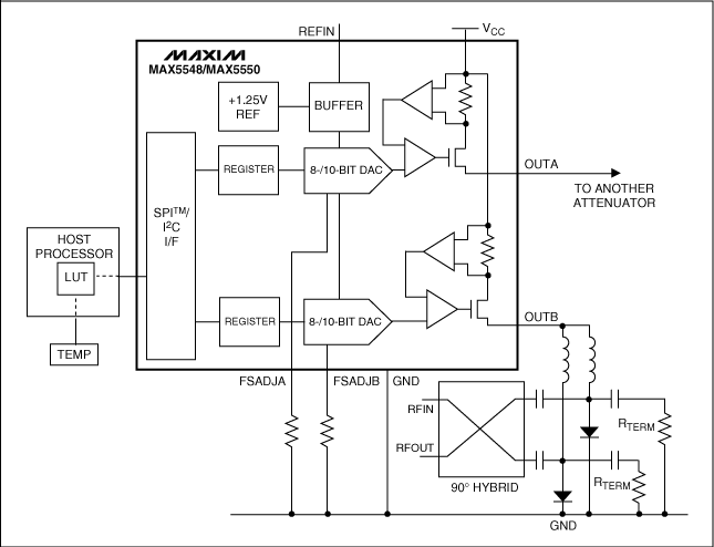
Figure 4. The RF attenuator is driven by a current output DAC (MAX5548 or MAX5550), which adjusts the output current according to the calibration signal of the host processor to perform temperature compensation. The output filter for the circuit with RF isolation inductance and capacitance (used to eliminate unwanted DC components), in the case of more than 100nH series inductance and 10nF capacitance to ground, the output can still maintain stability. The current output has an advantage over the voltage output in that if the voltage drop is within the DAC output voltage range, the series resistance introduced by the filter will not affect the accuracy. Appendix—DAC Example MAX5548 / MAX5550 is a dual-channel 8 / 10-bit DAC with a built-in current source output. The voltage range can reach 4V and the output current can reach 30mA. Both outputs can source up to 30mA, and can be used in parallel for high current circuits up to 60mA. This series of devices can operate from a single supply voltage of + 2.7V to + 5.25V. In normal operation mode, each DAC usually consumes 1.5mA of supply current, while in shutdown mode it is less than 1µA. In shutdown mode, the maximum output leakage current is only ± 1µA.
To ensure high accuracy and low noise performance, each IC has a + 1.25V bandgap reference and a control amplifier. You can also choose to connect an external reference (REFIN) to improve gain accuracy. The device is compatible with I²C and SPI serial interfaces and can be selected via pins. In SPI mode, the device can be connected in a daisy chain mode, thereby saving processor I / O pins; and for the I²C interface, four pin-selectable addresses are provided. The software and the external resistance corresponding to each output determine the maximum value of the programmable output current.
Phlizon COB series Grow Light, best full Spectrum designed to perfectly match large areas of indoor plants, hydroponics horticulture agriculture, and greenhouse, especially for indoor Plant.
3000K 5000K Cree COB and Epistar dual-chip,most efficient spectrum,high PPFD.Instead of having dozens of small diodes, COB style Led Grow Lights typically only have a handful of huge COBs, each with strong lenses to direct the light down into the plant.The big aluminum heat sink to protect the grow lights from high temperature,good cooling,long lifespan.Photosynthesis and promote healthy growth budding and flowering.
These are rapidly gaining in popularity and are known for having deep penetration into the plant canopy. 1000w/1500w/2000w /2500w /3000w COB light, they will give you more options when your plants need different strength of illumination.
2500W COB LED Grow Light,Phlizon COB Grow Light,Phlizon Cree COB Grow Light,Full Spectrum Cree COB Grow Light
Shenzhen Phlizon Technology Co.,Ltd. , https://www.philizon.com