Manufacturers of industrial or commercial energy-efficient fluorescent lighting products are faced with the pressure of the lighting device to have both advanced energy efficiency and small size. The new luminaires are available in a wide range of styles and are increasingly compact, allowing for enhanced control of ambient light settings at lower power levels. In addition, as long as the lighting products operate at low powers below 26W, there is no need to comply with power factor correction (PFC) requirements as large lamps. These have made small luminaires more attractive and have driven the development of miniature ballasts used to drive small luminaires. Among them, one of the main development directions of fluorescent lighting is dimmable lighting.
This article refers to the address: http://
As shown in Figure 1, a conventional ballast requires an input noise filter, a rectifier, and a smoothing capacitor to convert the AC voltage input to a DC power supply. They have a secondary circuit that produces a high frequency square wave voltage. This circuit consists of a control IC and a half bridge, and uses a resonant output stage to warm up, excite the fluorescent lamp and keep it working. If this design is to be added with dimming control, it is necessary to isolate the input and current sensing subcircuits to measure the current of the lamp. At the same time, a closed loop feedback circuit is used to compensate for the nonlinear characteristics of the lamp. This design greatly increases the number of components, cost, and space required for the solution, so the disadvantages are considerable.

Figure 1: Adding a dimmable circuit to a micro ballast.
Reduce device count, board area and cost
The situation has changed with more integrated IC solutions on the market. The latest development in this area is that with a highly integrated single device, the microballast can provide dimming without increasing the overall device size. International Rectifier (IR)'s IRS2530D DIM8 dimmable ballast control IC integrates the company's patented high voltage IC (HVIC) with its proprietary dimming method, allowing the entire ballast and dimmable circuitry to be included In an 8-pin SO8 package.

Figure 2: Block schematic of the IRS2530D.
Figure 2 shows a block diagram of the IRS2530D. A typical ballast operation occupies 6 of the 8 pins, 4 of which are used to supply the high-side and low-side MOSFET gate drivers (VB, HO, VS, LO). Therefore, manufacturers must adopt innovative methods to add dimming to their products. Therefore, the IR integrates the DC reference and AC lamp current, and provides a reference and feedback function for the closed loop dimming function through a pin. This innovative approach works well because designers use the new IC to design dimmable microballasts with fewer than 50 devices.
Operation and design
The state diagram of Figure 3 shows that this new IC transitions from UVLO mode to warm-up/trigger mode when VCC is first applied. When the integrated half-bridge oscillator starts at the highest frequency, the internal power supply to the VCO pin also begins to charge an external capacitor. As the frequency is gradually reduced to the resonant frequency of the circuit, the secondary winding of the resonant inductor will preheat the filament while the output voltage of the lamp will increase. When the voltage exceeds the trigger threshold voltage, the light will illuminate and the lamp current will begin to flow as the IC enters the DIM mode.
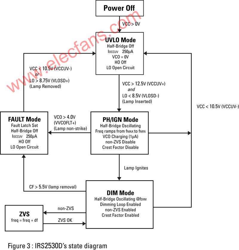
Figure 3: State diagram of the IRS2530D
Â
Designers must pay attention to the development of PCB layout precautions when designing circuits with this new IC. For example, they must maintain good interference suppression by ensuring that the design has the best performance; otherwise, even a properly connected circuit will fail due to poor device layout. Also, the best practices include maintaining proper creepage distances and clearances between high-voltage and low-voltage devices; keeping coupling capacitors close to their associated power supplies; and putting critical components as close as possible to their IC pins , achieve good interference filtering, and keep the dimmable feedback parts away from the high voltage conversion device as much as possible.
Other recommendations include the use of a dual filter on the power supply to isolate high current spikes that may be generated by the charge pump. It is also recommended to use a gate resistor to prevent Miller current from flowing back to the gate driver output. At the same time, it is also important to ensure that the COM node connection is implemented.
typical application
Figure 4 shows a typical circuit diagram. The AC output voltage in the figure has passed the full-wave rectification and EMI filter before being filtered by the DC bus capacitor. With IR's HVIC program, the IRS2530D can directly drive a half-bridge consisting of MHS and MLS to control preheat, excitation and lamp dimming voltage. This schematic also shows that the RVCC1 and RVCC2 resistors provide the IC's starting current, but whenever the half-bridge begins to vibrate, its operation is replaced by a charge pump consisting of CSNUB, DCP1, and DCP2. According to the previous recommendations, the power supply filter is provided by CVCC1, CVCC2, RLIM1 and RLIM2. On the other hand, the resonant circuits (LRES and CRES) bring the high voltage required for the lamp to trigger. This circuit also provides the low pass filtering required for lamp dimming. As for the DC blocking capacitor, that is, the CDC, it is responsible for preventing the lamp from blackening due to the migration of mercury, or shortening the life of the lamp.

Figure 4: Circuit diagram for a typical application.
The galvanically isolated 10VDC reference voltage applied to the DIM input in the design is provided by T1 and its associated devices and is biased on its secondary side by CVS, RVS1 and RVS2, so that its inputs and outputs can be tracked to each other. . The AC lamp current – ​​RCS across the current sense resistor is paired with the DIM pin by the CFB and RFB feedback circuits. In addition, other devices in the figure can enhance the protection design from shock, power failure or filament failure.
Additional design support
By applying its HVIC program and innovative design, IR has successfully developed a single wafer solution that accelerates the development of low power dimmable microballasts. To further simplify the design of the IRS2530D based on this new solution, IR also developed Ballast Design Assistant, which allows engineers to download and use it free of charge on IR's website, allowing them to take advantage of different linear input voltage ranges. , the type of light and the configuration of the lights, quickly designed for the target application. This software suite also provides the required ballast output data, IC programmable device values ​​and inductor specifications, as well as schematics and a complete bill of materials, which is a good help for designers.
Gas burner principle
The general use of stainless steel as the furnace material, through the electronic pulse ignition, the use of oil liquefied petroleum gas or natural gas combustion, heat to heat the above four independent high temperature crystal red gas heating plate and then baking food on the iron plate. With the energy-saving component control, the electronic pulse switch can also control the size of the flames to control the temperature of the iron plate, practical and convenient.Barbecue Grill, Gas Stove Burner, Windproof Camping Portable Stove, Gas Bbq Grill
Ningbo APG Machine(appliance)Co.,Ltd , http://www.apgelectrical.com