More and more devices need to access the network for remote control or resource sharing. The Ethernet interface is easy to route and has a wide communication bandwidth of up to 100 Mb/s or even 1000 Mb/s. Embedded systems are widely used in various electronic devices and industrial test equipment due to their small size, low price and high performance. With the increasingly tight integration of embedded systems and networks, the introduction of TCP/IP protocol stacks in embedded systems has become an important research direction in the field of embedded systems.
In this paper, based on the basic data transmission of the Ethernet interface, it is converted into other general-purpose serial interfaces (such as SPI, UART, CAN), which is more conducive to application in a wide range of industrial control fields. At present, most of the Ethernet control chips on the market have high power consumption and complex functions, and are not suitable for use in low-end embedded systems. The chip interface ENC28J60 from Microchip has only reached 10 Mbps, and its SRAM buffer is not easy to cause reception overflow. The ENC424J600 can reach 100 Mbps, the function will be more perfect, and provide two interfaces for embedded developers. Choice is a good network interface chip. STM32F103RET6 is an ARM processor with low power consumption, low price, powerful function, rich serial interface, 512 KB Flash, no need to expand Flash in general applications, it is low-end embedded. One of the best choices for developing systems. Combining the two not only enables network communication, but also can be flexibly converted into other serial interfaces for a wide range of uses.
Network controller peripheral hardware circuit
The ENC424J600 network controller peripheral hardware circuit design needs to pay attention to the following: The SPISEL pin of ENC424J600 needs to be pulled up to the power supply through a 100 kΩ resistor, so that the system can enter SPI mode when the system is powered up, and the INT pin is used as the receiving interrupt. A capacitor should be connected between each power supply pin and ground. In order to better prevent interference, two capacitors are added during the design. When wiring, the 0?01 μF capacitor is closer to the power supply pin; the RBIAS pin needs to be connected. A 12.4 kΩ resistor is connected to ground; in addition, the connection between the RD+ and RD-differential signals is different from that of a general network controller. It is not directly connected to the power supply through a resistor, and special care is required. The Ethernet interface adopts HR961160C, which integrates Ethernet isolation transformer and LED lamp into one body, and is also patch-type, saving PCB board space. When paying attention to the PCB layout, the traces of the two pairs of high-frequency differential lines of RD+, RD- and TD+, TD- should be symmetrical and as short as possible.
The peripheral hardware circuit of ENC424J600 and the peripheral circuit diagram of HANRUN Ethernet transformer socket are shown in Figure 2 and Figure 3.
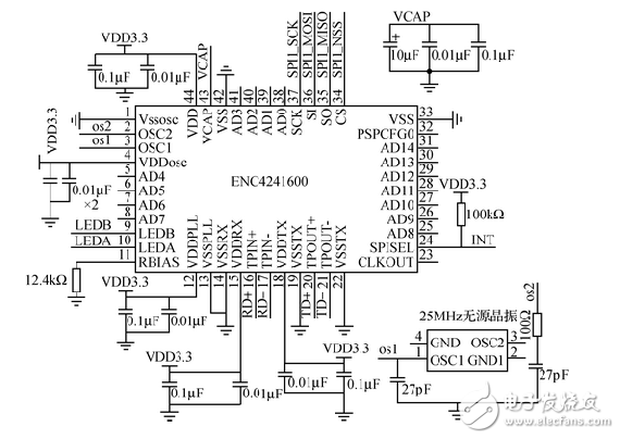
Figure 2 ENC424J600 peripheral hardware circuit
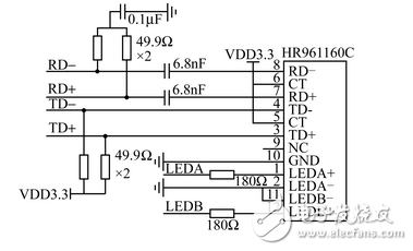
Figure 3 HANRUN Ethernet transformer socket peripheral circuit
The ENC424J600 is a separately available Fast Ethernet controller. It can be connected to the MCU using an industry standard serial bus SPI or a flexible parallel interface. The SPI interface has a data rate of up to 14 Mb/s and a parallel interface speed of up to 140 Mb/s. The ENC424J600 meets 10 baseTX full-duplex, half-duplex mode, 100 baseTX full-duplex, half-duplex mode, and all four modes are IEEE 802.3 compliant. The chip has a built-in PHY physical layer and a MAC media access control layer. The engine has RSA, DiffieHelman, AES, MD5, and SHA1 algorithms. The chip is available in 44-pin TQFP and QFN packages. Another outstanding feature of the chip is its 24 KB SRAM Buffer, which basically does not require an external SRAM. The chip SRAM Buffer is allocated as shown in Figure 1. The SRAM Buffer is divided into two areas. Generally, the General Purpose Buffer is set as the transmission area, the RX FIFO Buffer is set as the receiving area, and the two areas are distinguished by the pointer ERXST. Usually, the receiving area is set large to prevent the reception frame from overflowing.
Stud Triac is developed on the basis of common thyristors. It can not only replace two thyristors with reverse polarity in parallel, but also requires only one trigger circuit and is an ideal AC switch device. . Its English name TRIAC is the meaning of the triac.
China leading manufacturers and suppliers of Stud Triac,Ir Stud Triac, and we are specialize in Stud Type Triac,Sc108 Data Triac Stud, etc.

Stud Triac,Ir Stud Triac,Stud Type Triac,Sc108 Data Triac Stud
YANGZHOU POSITIONING TECH CO., LTD. , https://www.cndingweitech.com