IntroducTIonThis application note describes how to manage the internal data and program flash in the MAXQ7665 flash-based microcontrollers (µC) with page-erasable (PE) flash memory. This discussion includes general information for performing in-application programming (IAP) of the program flash. Memory MapsThis section details the general flash information and memory organization for various memory sizes of the MAXQ7665 µC family. There are three types of flash memory available on the MAX7665 devices: sector erase, single-word erase, and two-page erase. This document only covers MAXQ7665 devices with PE flash with two-page-erase data flash; the discussion does not apply to the sector-erase-only devices or to devices with single-word-erasable data flash. For information on MAXQ7665 sector-erasable (SE) devices, please refer to application note 3575, "In-Application Programming (IAP) of the MAXQ7665 Sector-Erasable Program and Data Flash". For information on MAXQ7665 PE devices with on e-word-erase data flash, please refer to application note 3579, "In-Application Programming (IAP) of the MAXQ7665 Page-Erasable (PE) Flash with One-Word-Erase Data Flash".
Table 1 through Table 3 show the memory maps for the 16KB device when executing code from program flash, utility ROM, and data SRAM respectively. Figures 1 and 2 chart the sector and page structure for the 16KB and 256B program flash. Other flash options are available; please consult the MAXQ7665 data sheet for a complete list.
Table 1. 16KB Memory Space—Executing from Program Flash
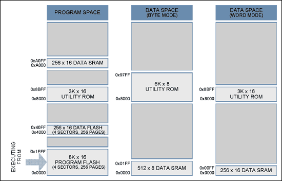
Table 2. 16KB Memory Space—Executing from Utility ROM
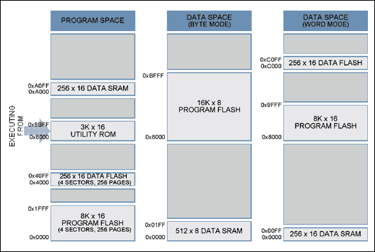
Table 3. 16KB Memory Space—Executing from Data SRAM
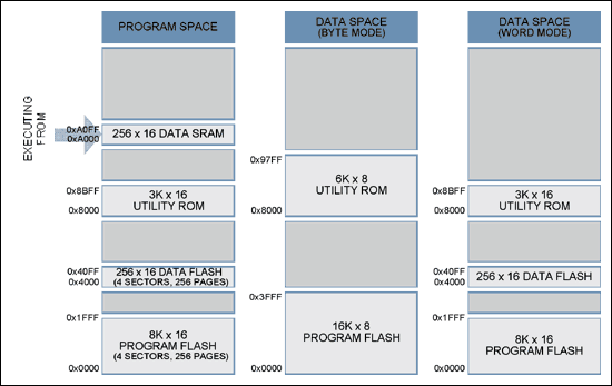
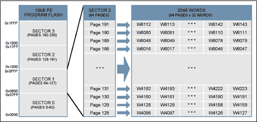
Figure 1. Sector / page structure for 16KB program flash.
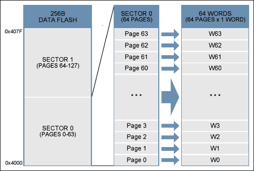
Figure 2. Sector / page structure for 256B data flash. Using Data Flash to Store Data The flash can be used to reliably store system data that needs to be programmed once or periodically during system operation. Unlike EEPROM, PE flash on the MAXQ7665 cannot be byte / word erased. Two pages must be erased at one time. This typically takes 10ms, but can take longer under worst-case conditions. During this time, the user code is stalled so no other processing can occur.
There are multiple techniques for storing data to flash, and several factors must be considered when you choose the appropriate method for your application. Does the application need to ensure that the current data remains intact until the new data is completely written? If the answer is yes, then some form of bank switching technique is necessary so the current data is not lost when newer data is written. How many erase / write cycles will occur during the life of the product? If the number of erase / write cycles will exceed the maximum specified in the data sheet, then using a bonded-queue approach can significantly increase the total erase / write cycles by spreading these cycles over multiple pages of the data flash. For most periodic data storage needs, bank switching and / or a bounded queue technique meets the reliability requirements and needs of the system. Simple examples of each technique follow. Bank SwitchingBank switching is an effective method of preventing data loss or corrupt ion during an erase / write cycle. This method works well by always maintaining at least one copy of the data. The drawback to bank switching is that it requires twice the amount of data flash than a bounded queue approach. Bank switching is, in fact , actually just the bounded-queue method with a queue size of 2. For this reason, please refer to the next section for details on how to implement a bounded queue. Bounded QueueA bounded queue is a queue limited by a fixed number of items and Commonly used whenever periodic data is processed. A bounded queue is formed by creating a fixed-length queue of "entries" equal to the desired data-block size. The entry size is application specific, and must be rounded up to the nearest page- erase boundary. Note: the minimum size that can be erased is two pages / words. While the data flash can be partitioned many ways based on application requirements, entries are limited to multiples of two pages due to the two-page-erase restriction imposed by the dat a flash. A 512 x 16 data flash, for example, can be divided into 32 16-word entries, which would result in the memory map in Table 4.
Upon initialization, a startup routine can scan the queue entries to determine the next available entry in the queue. Once the queue is full, it can be made to wrap back to the beginning. Once the data flash entry is erased, the new entry can be written. Figure 3 illustrates the flow of entries into a bounded queue.
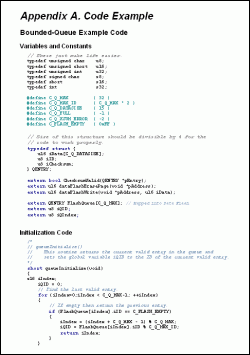
See Appendix A for a simple C source-code example.
Table 4. Example of a Bounded-Queue Memory Map
| FLASHQueue [] | |
| Queue Index | Data Flash Address |
| 31 | 0xC1F0-0xC1FF |
| 30 | 0xC1E0-0xC1EF |
| 29 | 0xC1D0-0xC1DF |
| ... | ... |
| 2 | 0xC020-0xC05F |
| 1 | 0xC010-0xC03F |
| 0 | 0xC000-0xC00F |
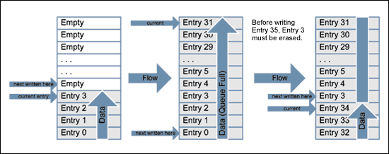
Figure 3. Diagram of a bounded queue flow. Utility ROM Flash RoutinesTo program, erase, and verify flash, the MAXQ7665 microcontroller has on-chip flash support routines residing in ROM (read-only memory). There are two ways to access these routines : direct access and indirect access through a lookup table. The fastest method is direct access, which is to directly call the routine. To do this, provide a header file with the following lines: u16 flashErasePage (void *); u16 flashEraseSector (void *); u16 flashEraseAll (void); u16 dataFlashWrite (u16 * pAddress, u16 iData); u16 dataFlashErasePage (void *); u16 dataFlashEraseSector (void *); u16 dataFlashEraseAll (void); Next, add linker defines to assign the appropriate address for each routine. For the IAR linker file, the added lines would look like this: -DflashEraseSector = 0x8XXX -DflashErasePage = 0x8XXX -DflashEraseAll = 0x8XXX Replace 0x8XXX with the appropriate memory address for each routine. Other compilers may use a different method for ad ding these references.
The flashWrite () utility routine cannot be called directly from C because of argument passing incompatibility with the C language. A small assembly routine like the one below must be written to call this function.
Note: the direct-access method does not provide forward compatibility with future ROM versions.
The second method is indirect access through a table lookup. This method provides greater compatibility with future ROM versions, but consumes more execution time. After each routine described below, an assembly routine uses the table-lookup method to obtain the address of the ROM Utility routine. Table 5 shows the flash routines supplied by the Utility ROM. For a complete listing of Utility ROM routines, please refer to the MAXQ7665 User's Guide.
Table 5. Flash Utility ROM Routines
| Routine Number | Routine Name | Entry Point ROMTable = ROM [800Dh] | Entry Point Physical Address |
| 1 | flashWrite | ROM [ROMTable] | 0x8XXX |
| 2 | flashErasePage | ROM [ROMTable + 1] | 0x8XXX |
| 3 | flashEraseAll | ROM [ROMTable + 2] | 0x8XXX |
| 4 | moveDP0 | ROM [ROMTable + 3] | 0x8XXX |
| 16 | flashEraseSector | ROM [ROMTable + 15] | 0x8XXX |
| 17 | dataFlashWrite | ROM [ROMTable + 16] | 0x8XXX |
| 19 | dataFlashErasePage | ROM [ROMTable + 18] | 0x8XXX |
| 20 | dataFlashEraseSector | ROM [ROMTable + 19] | 0x8XXX |
| twenty one | dataFlashEraseAll | ROM [ROMTable + 20] | 0x8XXX |
FlashWrite ()
| Routine: | u16 flashWrite (u16 * pDest, u16 * pSrc) |
| Summary: | Programs a single page (32 words) of program-flash memory. |
| Inputs: | DP [0] —Destination address in flash memory. DP [1] —Source address in SRAM holding 32 words of data to write. |
| Outputs: | Carry: Set on error and cleared on success. If set, then A [0] contains one of the following error codes: 1: failure due to software timeout 2: failure reported by hardware (DQ5 / FERR) 4: command not supported SW_FERR—Set on error, cleared on success. |
| Notes: | The watchdog must not be active or the watchdog timeout must be set long enough to complete this routine without triggering a reset. |
The following example of assembly code calls the flashWrite () utility routine using the indirect addressing method (lookup table). This routine is callable by C code.
; This routine is callable by C code using the following prototype; u16 flashWrite (u16 * pDest, u16 * pSrc);; flashWrite: move APC, # 0; No auto inc / dec of accumulator. Move AP, # 2; Set ACC to A [2]. move DP [0], # 0800Dh; This is where the address of the table is stored. move ACC, @DP [0]; Get the location of the routine table. add # 14; Add the index to the flashWrite routine. move DP [0], ACC move ACC, @DP [0]; Retrieve the address of the routine. push DP [1]; Save Frame Pointer on the stack. move DP [0], A [0 ]; Move argument 0 (dest address) to DP [0]. Move DP [1], A [1]; Move argument 1 (src address) to DP [1]. Call ACC; Execute the routine. Pop DP [1 ]; Restore Frame Pointer. Ret; Status returned in A [0]. FlashErasePage ()
| Routine: | u16 flashErasePage (void * pAddress) |
| Summary: | Erases a two-page block of program-flash memory. |
| Inputs: | A [0] —Address located in the two-page block to erase, ie, to erase pages 0 and 1, A [0] can contain any address from 0x0000 to 0x001F. |
| Outputs: | Carry: Set on error and cleared on success. If set, then A [0] contains one of the following error codes: 1: failure due to software timeout 2: failure reported by hardware (DQ5 / FERR) 4: command not supported SW_FERR—Set on error, cleared on success. |
| Notes: | The watchdog must not be active or the watchdog timeout must be set long enough to complete this routine without triggering a reset. |
; This routine is callable by C code using the following prototype; u16 flashErasePage (void * pAddress);; flashErasePage: move APC, # 0; No auto inc / dec of accumulator. Move AP, # 1; Set ACC to A [1 ]. move DP [0], # 0800Dh; This is where the address of the table is stored. move ACC, @DP [0]; Get the location of the routine table. add # 1; Add the index to the flashEraseSector routine . move DP [0], ACC move ACC, @DP [0]; Retrieve the address of the routine. call ACC; Execute the routine. ret; Status returned in A [0]. FlashEraseAll ()
| Routine: | Void flashEraseAll (void) |
| Summary: | Erases the entire program and data-flash memory. This routine can only be called from RAM. |
| Inputs: | None |
| Outputs: | Carry: Set on error and cleared on success. SW_FERR—Set on error, cleared on success. |
| Notes: | The watchdog must not be active or the watchdog timeout must be set long enough to complete this routine without triggering a reset. |
| Routine: | moveDP0 |
| Summary: | Reads a single word of flash memory. |
| Inputs: | DP [0] —Source address in flash memory. Add 0x8000 to read program flash. |
| Outputs: | GR will contain the data at specified address. |
| Notes: | This function cannot be called directly from C because the argument and return register are not compatible with C calling conventions. |
| Routine: | u16 flashEraseSector (void * pAddress) |
| Summary: | Erases a single sector of program-flash memory. |
| Inputs: | A [0] —Address located in the sector to erase. |
| Outputs: | Carry: Set on error and cleared on success. If set, then A [0] contains one of the following error codes: 1: failure due to software timeout 2: failure reported by hardware (DQ5 / FERR) 4: command not supported SW_FERR—Set on error, cleared on success. |
| Notes: | The watchdog must not be active or the watchdog timeout must be set long enough to complete this routine without triggering a reset. |
| Routine: | u16 dataFlashWrite (void * pAddress, u16 * pData) |
| Summary: | Programs a single word of data-flash memory. |
| Inputs: | A [0] —Word address in flash memory to which to write. A [1] —Word value to write to flash memory. |
| Outputs: | Carry: Set on error and cleared on success. If set, then A [0] contains one of the following error codes: 1: failure due to software timeout 2: failure reported by hardware (DQ5 / FERR) 4: command not supported SW_FER —Set on error, cleared on success. |
| Notes: | The watchdog must not be active or the watchdog timeout must be set long enough to complete this routine without triggering a reset. |
The following example of assembly code calls the dataFlashWrite () utility routine using the indirect addressing method (lookup table). This routine is callable by C code.; This routine is callable by C code using the following prototype; u16 dataFlashWrite (void * pAddress , u16 iData);; dataFlashWrite: move APC, # 0; No auto inc / dec of accumulator. move AP, # 2; Set ACC to A [2]. move DP [0], # 0800Dh; This is where the address of the table is stored. move ACC, @DP [0]; Get the location of the routine table. add # 16; Add the index to the flashWrite routine. move DP [0], ACC move ACC, @DP [0] ; Retrieve the address of the routine. Call ACC; Execute the routine. Ret; Status returned in A [0]. DataFlashErasePage ()
| Routine: | u16 dataFlashErasePage (void * pAddress) |
| Summary: | Erases two pages of data-flash memory. |
| Inputs: | A [0] —Address located in the two-page block to erase, ie, to erase pages 0 and 1, A [0] can contain address 0x4000 or 0x4001. |
| Outputs: | Carry: Set on error and cleared on success. If set, then A [0] contains one of the following error codes: 1: failure due to software timeout 2: failure reported by hardware (DQ5 / FERR) 4: command not supported SW_FERR—Set on error, cleared on success. |
| Notes: | The watchdog must not be active or the watchdog timeout must be set long enough to complete this routine without triggering a reset. |
| Routine: | u16 dataFlashEraseSector (void * pAddress) |
| Summary: | Erases a single sector of data-flash memory. |
| Inputs: | A [0] —Address located in the sector to erase. |
| Outputs: | Carry: Set on error and cleared on success. If set, then A [0] contains one of the following error codes: 1: failure due to software timeout 2: failure reported by hardware (DQ5 / FERR) 4: command not supported SW_FERR—Set on error, cleared on success. |
| Notes: | The watchdog must not be active or the watchdog timeout must be set long enough to complete this routine without triggering a reset. |
| Routine: | void dataFlashEraseAll (void) |
| Summary: | Erases the entire data flash memory. |
| Inputs: | None |
| Outputs: | Carry: Set on error and cleared on success. SW_FERR—Set on error, cleared on success. |
| Notes: | The watchdog must not be active or the watchdog timeout must be set long enough to complete this routine without triggering a reset. |
The Utility ROM flash routines outlined in the previous section perform all the actions necessary to erase and write the flash ROM. It is thus possible for an end-user application to perform operations on the flash memory. Like any other subroutine call, control will return to the end-user's code after completion of the routine.
For a reliable IAP the boot-loader application must be separate from the main application. This ensures that the reprogramming procedure can be retried even after an incomplete reprogramming sequence occurred. Boot LoaderThe ROM jumps to address 0x0000 after initialization. The entry point of the boot -loader application must, therefore, be placed at 0x0000. The boot-loader application can extend into as many flash sectors / pages as needed, but any page used will not be available for the user's application code. The specific requirements that must be met when erasing and writing flash are listed in Table 6.
Table 6. Requirements for Calling Flash Utility ROM Routines
| You cannot erase or program from the same flash page from which you are executing code. This is not normally a problem since the flash boot-loader application should never be erased during IAP. |
| The watchdog must not be enabled, or the watchdog timeout must be set long enough to complete this routine without triggering a reset before calling the flashEraseSector () or flashErasePage () routine. If the watchdog time out occurs before the erase is complete, it will reset the part. |
| Because the System Control Register bit, SC.UPA, must be set to 0 to access the Utility ROM, a Utility ROM routine cannot be called directly from program memory addresses ≥ 0x8000. If access to a Utility ROM routine is required from a program in upper memory (≥ 0x8000), the program must in directly call the ROM routine through a routine residing in lower memory (<0x8000). This restriction effectively limits the boot loader to = 64KB (32KB x 16). |
The flowchart in Figure 4 shows what the MAXQ7665 does when exiting the reset state. After a diagnostic of the ROM itself and verification that the flash is ready, the ROM initialization code jumps directly to address 0x0000.
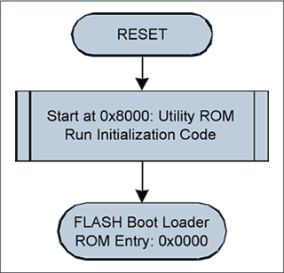
Figure 4. Flowchart of a simplified ROM initialization.
The Figure 5 flowchart shows how a simple boot-loader application can function. A simple application header might look something like: typedef struct {u16 iSize; // The size of the application in words u32 iCRC; // The CRC of the application u8 ID [8]; // ID string for current application} APPLICATION_HEADER; Using the information from this header, the boot loader can check the validity of the main application program and report the version identification if requested.
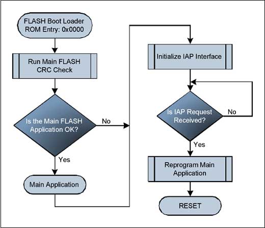
Figure 5. Flowchart for a simplified flash boot loader.
The programming sequence itself is quite simple. Erase each sector / page containing the main application code through a call to flashEraseSector () and / or flashErasePage (). Then write one page at a time by calling flashWrite () for every 32 words that need to be programmed. We advise you to erase the page containing the application header first, and program the CRC data last to minimize the possibility of an errant CRC match. A very simple routine to reflash the microcontroller that gets data through the serial port can look like the following:
/ * // VerySimpleReFlash () // As simple as it gets. // Step 1. Wait for erase command, then erase flash. // Step 2. Wait for program command, program flash one word at a time. * / Void VerySimpleReFlash () {u16 iStatus; // The status returned from flash utility ROM calls s32 iSize; // The size of the main code to program u16 * pAddress = 0x2000; // The starting address of the main application u16 i; InitializeCOMM ( ); // Can be CAN or UART. WaitForEraseCommand (); // Assume that application starts at the beginning of a sector. For (i = C_START_SECTOR; i 0) {u16 iData [32]; Get32WordsFromCOMM (iData); iStatus = flashWrite (pAddress, iData); if (iStatus) break; pAddress + = 32; iSize-= 32; UpdateWatchdog (); // Prevent timeout} SendFlashWriteResponse (iStatus); ResetMicro ();} Appendix A. Code Example
Download (DOC 33kB)
Sijee Fiber optic adaptors are part of passive components for FTTH ODN connectivity, Sijee Fiber optic adaptors are used to join two fiber optic patch cables together for realizing the transition between different interfaces and they are available for use with either single-mode or multimode Fiber Optic Patch Cord. Sijee Fiber optic adaptors can offer superior low loss performance with very high repeatability.
Sijee offers different types of fiber adaptors comply with ITU standard, main products including Fiber Mating Sleeve Adaptor, Fiber Hybrid Adaptor, Fiber Bare Fiber Adaptor , Fiber Mechanical Attenuator, Field Assembly Optical Connector (FAOC), Splice-On Connector, Semi-finished Fiber Connector, etc.
Optical Fiber Couplers,Optical Fiber Adapter,Fiber Optic Adapter, Fiber Optic Flange are available.
Features:
1. Compliant with: IEC, JIS, Telcordia
2. Convenience and ease of handling
3. Optical performance 100% factory tested
4. Flange or threaded mounting type
5. Ceramic/Zirconia or phosphorous bronze sleeves
6. Good changeability and repeatability
Applications:
1. Telecommunication networks
2. FTTX, FTTH
3. LAN, WAN, CATV networks
4. Fiber communications, Data communication networks and processing, Industrial, Mechanical and Military.
5. Active device termination


Fiber Adaptor
Optical Fiber Couplers,Optical Fiber Adapter,Fiber Optic Adapter,Fiber Optic Flange
Sijee Optical Communication Technology Co.,Ltd , https://www.sijee-optical.com