Introduction Microchip's PICmicro microcontroller (PIC) has become the mainstream choice for low-power, low-cost system solutions. These microprocessors have multiple general-purpose input and output pins (GPIO). By simply combining these pins, the 1-Wire protocol of Dallas Semiconductor can be realized. Various Dallas Semiconductor devices including iButton® work in coordination. This application note gives a 1-Wire communication subroutine based on PIC16F628, and introduces its timing and other related contents in detail. For convenience, all clock frequencies are assumed to be 4MHz. Everyone knows that this frequency is also the internal clock frequency of many PICs. Appendix A is a file included in all these subroutines, and Appendix B is a piece of assembly language code that PIC16F628 reads data from the high-precision lithium battery monitor DS2761. One thing to note here is that this application note is only suitable for normal speed 1-Wire communication. For the implementation of the 1-Wire protocol on the host side of the general macro command, GPIO only needs two states, namely the high-impedance state and the logic low level. The following small assembly procedure is used to achieve this function. PIC16F628 has two sets of GPIO ports: PORTA and PORTB, any of which can be used to complete 1-Wire communication. In this example, PORTB is selected, and a constant DQ is also configured in the assembly code, which is used to set which bit of PORTB is used as the 1-Wire pin. Throughout the code, this bit is simply referred to as DQ. Outside the circuit, this pin should be connected to the positive terminal of the power supply through a pull-up resistor. OW_HIZ: MACRO; Force the DQ line into a high impedance state. BSF STATUS, RP0; Select Bank 1 of data memory BSF TRISB, DQ; Make DQ pin High Z BCF STATUS, RP0; Select Bank 0 of data memory ENDM OW_LMACRO; Force the DQ line to a logic low. BCF STATUS, RP0; Select Bank 0 of data memory BCF PORTB, DQ; Clear the DQ bit BSF STATUS, RP0; Select Bank 1 of data memory BCF TRISB, DQ; Make DQ pin an output BCF STATUS, RP0; Select Bank 0 of data memory ENDM These two codes are written as macro instructions. Write them as macro instructions, and insert them automatically by calling a macro instruction in the assembly source code, thus reducing the number of code rewriting. The function of the first macro instruction OW_HIZ is to force DQ to high impedance state. Since the TRISB register is located in bank 1 of the data memory, the first step is to select bank 1 of the data memory. Then, by setting the DQ bit in the TRISB register, the DQ output driver becomes high impedance. The last line of the code changes back to bank 0 of the data memory. The last line is not necessary, but it is still added here so that the data memory is in a certain state after all macro instructions and function calls.
The function of the second macro instruction OW_LO is to force DQ to low level. First select bank 0 of the data memory so that the PORTB register is addressed. The PORTB register is a data memory. When set as an output, it contains the forced output values ​​of those configured as output pins in TRISB.
Clear the DQ bit of PORTB so that the lead is forced low. Finally, select bank 1 of the data register and clear the DQ bit of the PORTB register to use it as an output driver. As with the other, the macro instruction ends with the selection of bank 0 of the data memory.
The final macro instruction WAIT is used to generate the delay required for 1-Wire signaling. WAIT can generate delay times that are integer multiples of 5µs. In this macro, first simply calculate the required multiple of the 5µs delay, and then do the corresponding number of cycles in WAIT5U. The WAIT5U subroutine will be discussed in the next section. For each instruction in WAIT, the processing time used is annotated to facilitate the understanding of how the delay is realized. WAIT: MACRO TIME; Delay for TIME µs .; Variable TIme must be in mulTIples of 5µs. MOVLW (TIME / 5 )-1; 1 µs to process MOVWF TMP0; 1 µs to process CALL WAIT5U; 2 µs to process ENDM 1-Wire general subroutine In order to ensure successful communication, the 1-Wire timing protocol has some special timing restrictions that must be observed. To facilitate the generation of special delays, the subroutine WAIT5U can be used to generate a delay of 5µs. This subroutine is as follows: WAIT5U:; This takes 5µs to complete NOP; 1µs to process NOP; 1µs to process DECFSZ TMP0, F; 1µs if not zero or 2µs if zero GOTO WAIT5U; 2µs to process RETLW 0; 2µs to process The program can be used together with WAIT macros to generate commonly used delays. For example, if a delay of 40µs is required, WAIT 0.40 is called. Run the first 3 lines of WAIT first to generate a delay of 4µs, then run the first 4 lines of WAIT5U 6 times, each time to generate a delay of 5μs, the total delay is 30μs, the last round of WAIT5U needs 6μs, and then return to WAIT macro, so the total processing time is 30 + 4 + 6 = 40µs.
Table 1. 1-Wire interface timing requirements at standard speed
| 2.5V <VDD <5.5V, TA = -20 ° C to 70 ° C | |||||
| Parameter | Symbol | Min | Typ | Max | Units |
| Time Slot | tSLOT | 60 | 120 | µs | |
| Recovery Time | tREC | 1 | µs | ||
| Write 0 Low Time | tLOW0 | 60 | 120 | µs | |
| Write 1 Low Time | tLOW1 | 1 | 15 | µs | |
| Read Data Valid | tRDV | 15 | µs | ||
| Reset Time High | tRSTH | 480 | µs | ||
| Reset Time Low | tRSTL | 480 | 960 | µs | |
| Presence Detect High | tPDH | 15 | 60 | µs | |
| Presence Detect Low | tPDL | 60 | 240 | µs | |
All processes of 1-Wire communication start with a reset pulse sent by the master, followed by the slave's response detect pulse. Figure 1 illustrates this transaction. The initialization sequence can be issued through PIC, it is very simple, the corresponding assembly code is shown in Figure 1. The timing parameters of initialization, read operation, and write operation are listed in Table 1. These parameters will also be referenced later in this article.
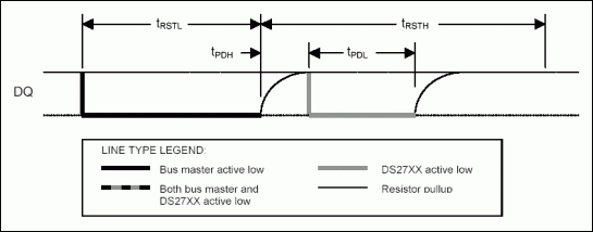
Figure 1. 1-Wire initialization sequence OW_RESET: OW_HIZ; Start with the line high CLRF PDBYTE; Clear the PD byte OW_LO WAIT .500; Drive Low for 500µs OW_HIZ WAIT .70; Release line and wait 70µs for PD Pulse BTFSS PORTB, DQ; Read for a PD Pulse INCF PDBYTE, F; Set PDBYTE to 1 if get a PD Pulse WAIT .430; Wait 430µs after PD Pulse RETLW 0 The OW_RESET subroutine starts from ensuring that the DQ pin is in a high-impedance state so that it can pass The pull-up resistor pulls DQ high. Then clear the PDBYTE register, so that it is ready for the subsequent presence detection pulse. After that, DQ goes low for 500µs, which meets the requirements of the tRSTL parameter in Table 1, while leaving 20µs extra buffer time. After turning this pin to low level, it returns to the high impedance state, and a delay of 70µs is added before reading the in-position detection pulse. This 70µs delay ensures that no matter how tPDL or tPDH changes, the PIC can always sample at the effective time. Once the presence detection pulse is read, the PDBYTE register is set to the logic state value that has been read. The DQ pin is kept in a high-impedance state for 430µs to ensure that tRSTH is met, and 20µs of extra buffer time is allowed.
Another subroutine required for 1-Wire communication is DSTXBYTE, which is used to send data to a 1-Wire slave device. The PIC code of this subroutine is shown in Figure 2. This subroutine needs to be called with the data to be sent in the WREG register. First put the data to be sent into the IOBYTE register immediately, and then initialize the COUNT register to 8 to count the bits to be sent on the DQ port line. Starting from DSTXLP, PIC sends data. Regardless of whether the transmitted level is high or low at the beginning, the DQ pin goes low for 3µs, which meets the requirements of tLOW1. Then the LSB of IOBYTE is shifted to the CARRY bit, and then it is checked whether it is 0 or 1. If CARRY is 1, the DQ bit of TRISB is set, the pin becomes high impedance, and the line is pulled high by the pull-up resistor. If CARRY is 0, the line remains low. After that, a delay of 60µs was introduced to allow normal operation when tLOW0 is at the minimum value. After a 60µs wait, the pin becomes high impedance, followed by an additional delay of 2µs for the pull-up resistor to recover. Finally, COUNT decreases by 1. If the value of the COUNT register becomes 0, it means that all data has been sent and the subroutine ends. If the value of the COUNT register is not 0, continue to send the next bit of data from DSTXLP. Refer to Figure 2 for how to write 0 or 1 in the program.
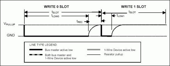
Figure 2. 1-Wire write timing DSTXBYTE:; Byte to send starts in W MOVWF IOBYTE; We send it from IOBYTE MOVLW .8 MOVWF COUNT; Set COUNT equal to 8 to count the bits DSTXLP: OW_LO NOP NOP NOP; Drive the line low for 3µs RRF IOBYTE, F BSF STATUS, RP0; Select Bank 1 of data memory BTFSC STATUS, C; Check the LSB of IOBYTE for 1 or 0 BSF TRISB, DQ; HiZ the line if LSB is 1 BCF STATUS, RP0; Select Bank 0 of data memory WAIT .60; Continue driving line for 60µs OW_HIZ; Release the line for pullup NOP NOP; Recovery time of 2µs DECFSZ COUNT, F; Decrement the bit counter GOTO DSTXLP RETLW 0 The last child of 1-Wire communication The program is DSRXBYTE, the main function is to receive information from the slave device, and its code is shown in Figure 3. Before the DQ takes action, first initialize the COUNT register to 8, indicating the number of bits to be received. At the beginning, DSRXLP first turns the DQ pin to a low level and sends a signal to the slave device, indicating that it is ready to receive data. This line is kept low for 6µs, and the port line is released by setting the DQ line to a high-impedance state, and then the PIC waits another 4µs before sampling the data line. When the line level goes low, there is 1 line of code in OW_LO and 3 lines of code in OW_HIZ. The processing time of one line of code is 1µs, and all the time is 1 + 6 + 3 + 4 = 14µs, which is just lower than the tRDV of 15µs. After PORTB is read, the DQ bit is masked. This register performs addition until 255, forcing the CARRY bit to mirror the DQ bit, and then CARRY shifts the bit to the IOBYTE that holds the received data. Once this byte is stored, a delay of 50 µs is required to ensure that the tSLOT requirement is met. The final check is to determine whether the COUNT register is zero. If it is zero, it means that 8 bits have been read and exit the subroutine; otherwise, go to DSRXLP and repeat the cycle. The process of reading 0 and reading 1 is shown in Figure 3.
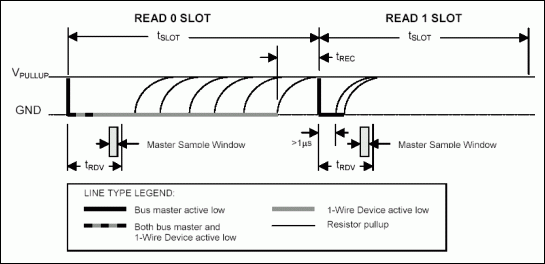
Figure 3. 1-Wire read slot DSRXBYTE:; Byte read is stored in IOBYTE MOVLW .8 MOVWF COUNT; Set COUNT equal to 8 to count the bits DSRXLP: OW_LO NOP NOP NOP NOP NOP NOP; Bring DQ low for 6µs OW_HIZ NOP NOP NOP NOP; Change to HiZ and Wait 4µs MOVF PORTB, W; Read DQ ANDLW 1 <
Appendix A: 1-Wire contains FILE (1W_16F6X.INC); ************************************ *******************;; Dallas 1-Wire Support for PIC16F628;; Processor has 4MHz clock and 1µs per instruction cycle.;; ******** ***********************************************; ** ************************************************** ***; Dallas Semiconductor 1-Wire MACROS; *************************************** **************** OW_HIZ: MACRO BSF STATUS, RP0; Select Bank 1 of data memory BSF TRISB, DQ; Make DQ pin High Z BCF STATUS, RP0; Select Bank 0 of data memory ENDM; ----------------------------------------------- --------- OW_LMACRO BCF STATUS, RP0; Select Bank 0 of data memory BCF PORTB, DQ; Clear the DQ bit BSF STATUS, RP0; Select Bank 1 of data memory BCF TRISB, DQ; Make DQ pin an output BCF STATUS, RP0; Select Bank 0 of data memory ENDM; ------------------------------------ -------------------- WAIT: MACRO TIME; Delay for TIME µs.; Variable time must be in multiples of 5µs. MOVLW (TIME / 5) -1 ; 1µs MOVWF TMP0; 1µs CALL WAIT5U; 2µs ENDM; ************************************** *****************; Dallas Semiconductor 1-Wire ROUTINES; ************************* ****************************** WAIT5U:; This takes 5µS to complete NOP; 1µs NOP; 1µs DECFSZ TMP0, F; 1µs or 2µs GOTO WAIT5U; 2µs RETLW 0; 2µs; --------------------------------------- ----------------- OW_RESET: OW_HIZ; Start with the line high CLRF PDBYTE; Clear the PD byte OW_LO WAIT .500; Drive Low for 500µs OW_HIZ WAIT .70; Release line and wait 70µs for PD Pulse BTFSS PORTB, DQ; Read for a PD Pulse INCF PDBYTE, F; Set PDBYTE to 1 if get a PD Pulse WAIT .400; Wait 400µs after PD Pulse RETLW 0; --------- ----------------------------------------------- DSRXBYTE:; Byte read is stored in IOBYTE MOVLW .8 MOVWF COUNT; Set COUNT equal to 8 to count the bits DSRXLP: OW_LO NOP NOP NOP NOP NOP NOP NOP; Bring DQ low for 6µs OW_HIZ NOP NOP NOP NOP; Change to HiZ and Wait 4µs MOVF PORTB , W; Read DQ ANDLW 1 <
Anti-Scald Electric Kettle
Help you to boiled water in 5 minutes. 201stainless steel Electric Kettle which have passed food grand with a sleek and anti-Scald design and will compliment your kitchen counter-top to the fullest. It is equipped with a long handle that can be used by people of all hand sizes without straining your wrists anymore. Allow you to heat water faster than a microwave oven and surely safer than a stovetop kettle.
Features:
· Anti-Scald Electric Kettle: Protect your hand for avoid the scald. When you touch the body, it will not hurt you. Fill it more from the max line. We got you covered for a great and fast Anti-Scald Electric Kettle in the market, Besides the great and nice design, this kettle is extremely durable and will provide you endless coffee moments with family and friends and for your morning.
· High Quality Stainless Steel Teapot: Forget all about cheaply made electric kettles and trust your coffee or tea with our durable Stainless Steel Kettle. Keep one at the house, one at the office and one for your camping explorations to enjoy your coffee and tees.
· Anti-Scald Handle For Easy Holding & Using: Upon designing this electric teapot, we tried to make it extremely easy and convenient to use. Place your hand around the handle when the water is ready, lift the cordless kettle and pour some hot water in your cup.
· Fast Heating & Automatic Shut Off: Our Anti-Scald Electric Kettle kettle has an automatic shut off button, so as to keep you safe when the water is ready.
· 360 Degree Rotational body with separated base: A 360-degree swivel ensures that you can pick it up from any side. Just plug it in and place it on your kitchen counter so that everyone in your family can pour themselves a steaming cup or water for their tea or coffee.
Application:
Make your favourite coffee.
Prepare comforting hot chocolate.
Cook eggs.
Anti-Scald Electric Kettle
Anti-Scald Electric Kettle,Plastic Handle Kettle,Stainless Steel Kettle,Professional Electric Kettle
Guangzhou Taipeng Electrical Appliances Technology CO., LTD. , https://www.taipengelectric.com