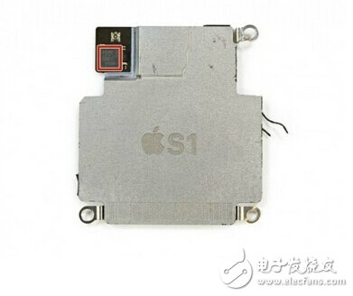
The Apple Watch is powered by an S1 chip. It has 30 separate components in a 26mm & TImes; 28mm chip, which is absolutely "amazing". It also includes NXP's NFC chip, AMS's NFC signal amplifier, and Maxin's audio amplifier. Today, foreign media is working with us to understand this chip from a more professional perspective. Many OEMs currently developing and selling smart watches are smart phone manufacturers, so we will see that these manufacturers usually directly plug the components of the smart phone into the smart watch.
Many Android Wear watches use the Qualcomm Snapdragon 400 chip for modems. The A7 chip is suitable for smart watches from the perspective of thermal design power consumption. The Android Wear watch has a battery capacity of about 400 mAh and can last for 1-2 days, but for the market these watches are too big, so you need a SoC system-on-chip designed specifically for the shape and size of smart watches.
For the Apple Watch S1 chip, there is currently no suitable running test tool, but we can see from the disassembly of this device that the SoC uses the Samsung 28nm LP process, and only the HKMG or poly SiON gate can be used. structure. Selecting different structures will also have different power efficiencies because the leakage power of the HKMG process is smaller. Compared with the cost of using the 20/14nm process, the cost difference between the two processes is not large. In addition, TSMC's impact on battery life after switching from 28LP process to 28HPm on Snapdragon 600 and 800 chips can basically determine Apple's This chip uses the HKMG process.
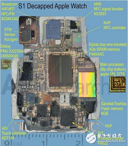
We also know that the binary is compiled for the ARMv7k processor of the watch, but unfortunately there is no relevant record about the architecture of the instruction set. watchOS was developed on the basis of iOS/Darwin, which means that in order to obtain storage protection and key abstractions, such as virtual memory, it needs the memory management unit MMU, which eliminates the possibility of using MCU ISA like ARMv7m. We suspect that Apple may be using a derivative ARMv7-A to streamline unnecessary instructions to reduce power consumption.
As for the GPU of the device, it is not so mysterious. From the PowerVR drive that appears in the Apple Watch, the S1 may use the PowerVR Series 5 GPU. Which one is not clear, it may be the PowerVR SGX543MP1. However, I prefer the PowerVR GX5300 because it is a GPU optimized for wearable devices and uses the same drivers. But no matter what, before the arrival of watchOS 2, Apple Watch can't run the application natively. We can dig into it very little, and even if watchOS 2 is released, the graphics running score may not be good.
Next, let's take a look at the CPU's hierarchical memory architecture, which is a very important piece of information for applications that need to be optimized to ensure that the code has enough time and/or spatial locality to guarantee code performance.
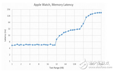
As shown in the figure, there is a very large fluctuation between DRAM 28KB and 64KB. Since we have cleared the local maximum of the L1 data cache, we can basically determine the L1 data cache size is 32KB, which is currently on the market for many products. The L1 data cache is also between 32 and 64KB. And there is a big change again in the 224KB or so, we can also determine that L2's data cache is 256KB, which is much smaller than the current 1-2MB shared cache of large smartphone CPUs, but it is just right compared with A5 or A7. .
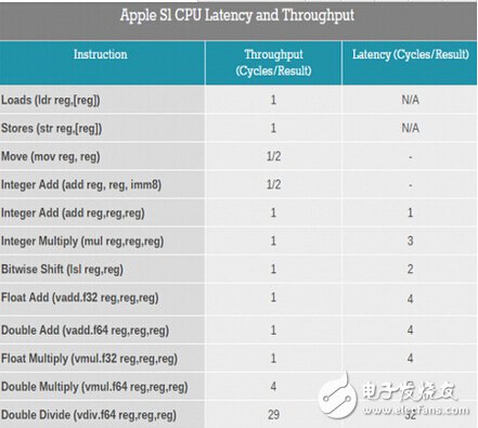
The maximum CPU frequency of the Apple Watch is 520 MHz. Let's take a look at its architecture. In terms of integer arithmetic, the integer addition delay is one loop, and the integer multiplication delay is three loops. But because the throughput of the pipeline integer multiplication can output a clock cycle result. The same bit shift takes two cycles to complete, while throughput takes only one clock cycle. The multiplication and addition interleaving throughput will be only half. We can guess that this is because the integer addition block is the same as the integer multiplication block, but this doesn't make much sense, because at the logical level, the addition and multiplication are too different.
From a data type perspective, integers are just one factor, as well as booleans, characters, strings, and integers of different sizes, but when it comes to decimal, the application still uses floating point to compile. Like this low-power CPU, floating point is usually slower than integers, because the rules of floating-point arithmetic are more complicated.
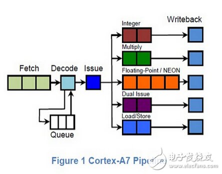
If the latency and throughput time of the web page you open is for Cortex A7, you might guess that it is Cortex A7, then you probably guessed it. Loading storage at the same time means that these are XOR operations and cannot be performed in parallel. The same is true for multiplication and addition. Although Cortex A7 and Cortex A5 have the same point, it does not explain why it is possible to add two immediate/constant values ​​and accumulate registers per clock cycle.
From this data we can be sure that it is a single core Cortex A7. Although it is only the Cortex A7, the maximum clock speed is low, which means that the logic design pays more attention to power efficiency than performance. Standard batteries can take advantage of certain technologies and styles that actually affect the performance of 2+ GHz chips, but are well suited for use in 520 MHz chips. The Cortex A7 is a benefit in terms of energy efficiency and performance. Perf/W (Performance per Watt), so I think the key difference in the future will be the implementation method, not the architecture. Although I also hope that Apple Watch can use more advanced processes, such as 14LPP/16FF+, there is basically no such possibility before the second or third generation of Apple Watch.
100W Wall Pack Lights,Wall Pack Light Fixture,Wall Pack Light 100W,LED Wall Pack Light 140Lm/W
Vietnam JJ Lighting Company , https://www.vnjjlighting.com