Introduction In order to achieve the best performance of a high-speed digital-to-analog converter (DAC), it is necessary to strictly meet the timing requirements of digital signals. As the clock frequency increases, the establishment and hold time of the digital interface becomes a parameter that system designers need to focus on. This application note describes the setup and hold time in detail, because these parameters are closely related to Maxim's high-performance data conversion solutions.
Definition Setup and Hold Time Setup time (tS) is the time that the data must reach a valid logic level relative to the DAC clock transition. Hold time (tH) defines the time allowed for the data to change after the device captures / samples the data. Figure 1 shows the setup and hold times relative to the rising edge of the clock. The effective edge of the clock signal for a particular device may be a rising / falling edge, or selected by the user, such as the MAX5895 16-bit, 500Msps, interpolation and modulation dual-channel DAC, CMOS input.
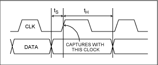
Figure 1. Setup and hold time relative to the rising edge of the clock signal
Digital circuits designed with CMOS technology usually use the intermediate value of the power swing as the switching point. Therefore, the time reference point is set at the midpoint of the signal edge. The waveform in Figure 1 indicates the setup and hold time of the device under typical conditions. Note that these two parameters defined at this time are positive values, but will be confusing when a negative value occurs during the setup or hold time.
The MAX5891 600Msps, 16-bit DAC provides a good learning example for this intermediate value state. The device has a settling time of -1.5ns and a hold time of 2.6ns. Figure 2 shows the minimum settling time of the MAX5891. Note that in actual applications, data usually changes after the sampling clock transitions. Figure 3 shows the minimum hold time for the same device.
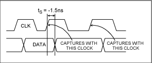
Figure 2. MAX5891 minimum settling time
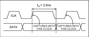
Figure 3. MAX5891 minimum hold time
To meet these requirements, users need to analyze the transmission delay and jitter of the data source. The propagation delay determines the nominal timing requirements of the clock, and the jitter index determines the allowable tolerance. To explain this relationship, we take a logic gate circuit with a transmission delay of 1.5 ns as an example. If the same clock signal is used in the logic gate circuit, the MAX5891 will just meet the settling time shown in Figure 2. In this case, there is no design margin for temperature drift, clock or data jitter, and differences between devices.
Two methods can be used to optimize the setup and hold time, including increasing the clock delay and maintaining a consistent lead length. Increasing the clock delay between the data source and the DAC helps solve the transmission delay problem in the above example. Maintaining a consistent lead length between the data source and the DAC input pin can ensure that jitter and drift will not cause a bit to enter the next clock cycle. It should be noted that we are dealing with a high-speed data bus containing multiple data lines, and all bits must meet the timing requirements at any time.
Conclusion The timing of processing high-frequency data faces many challenges. Solving these problems requires designers or system design engineers to fully understand the specifications of all devices in a specific signal chain. If the specifications of any device in the link are not met, the system performance will be reduced. The performance degradation manifests itself as a decrease in DAC output accuracy or limits the clock frequency.
19V Plug in wall charger with interchangeable plugs, AC DC Switching Power Adapter with detachable AC plug, universal adapter, switching interchangeable power supply, interchangeable power supplies,19V Detachable Plug Power Adapter with 6 different plugs types (CN, USA, EU, KR,AU and UK).
19V detachable plug power adapter for tablet, bluetooth speaker, massage chair, humidifier, juice extractor, coffee machine, small household appliance, fingerprint scanner, CCTV camera-etc.
With these 6 interchangeable plugs -- CN,KR,US,EU,AU,UK plug, you can only take one 19V plug in wall power adapter with you when you traveling among these 6 countries.
We can also make it with more plugs if you tell us your specific requirement.


19V Detachable Plug Power Adapter
19V Detachable Plug Power Adapter,Detachable Plug Power Adapter
Shenzhen Juyuanhai Electronic Co., Ltd. , https://www.powersupplycn.com