DDS is the acronym for Direct Digital Synthesizer and is a key digital technology. Compared with traditional frequency synthesizers, DDS has the advantages of low cost, low power consumption, high resolution and fast switching time. It is widely used in telecom and electronic instruments and is a key technology to realize the full digitalization of equipment.
The DDS chip mainly includes three parts of frequency control register, high-speed phase accumulator and sine calculator (such as Q2220). The frequency control register can load and register the frequency control code input by the user in serial or parallel mode; the phase accumulator is based.

The frequency control code performs phase accumulation in each clock cycle to obtain a phase value; the sine calculator calculates the digital sine wave amplitude for the phase value (the chip is generally obtained by looking up the table). The output of the DDS chip is generally a digital sine wave, so a high-speed D/A converter and a low-pass filter are required to obtain a usable analog frequency signal.
What are the advantages of DDS?
High frequency resolution, multiple output frequency points, up to 2 N-th power frequency points (N is the number of phase accumulators); frequency switching speed is fast, up to us-level; frequency switching is continuous; frequency can be output Orthogonal signal; low output phase noise, improve the phase noise of the reference frequency source; can generate arbitrary waveforms; fully digital implementation, easy to integrate, small size, light weight.
The AD9850 is a direct frequency synthesizer manufactured by AD Corporation with a maximum clock of 125 MHz and advanced CMOS technology. It is mainly composed of a programmable DDS system, a high-performance digital-to-analog converter (DAC) and a high-speed comparator. Frequency synthesis of digital programming control.
The AD9850 uses Direct Digital Synthesis (DDS) technology with a programmable DDS system and high-speed comparator for full digital programming controlled frequency synthesis. The core of the programmable DDS system is the phase accumulator, which consists of an adder and an N-bit phase register. N is typically 24-32. For each external reference clock, the phase register is incremented by the step size M. The output of the phase register is added to the phase control word and can be input to the sine lookup table address. positive
The string lookup table contains digital amplitude information for a sine wave period, each address corresponding to a phase point in the range of 0° to 360° in the sine wave. The lookup table maps the phase information of the input address to a sine wave amplitude signal and then drives the DAC to output the analog quantity.
Production process and processA source is required for any transmitter or receiver. This source can be an RC oscillator, an LC oscillator, a crystal oscillator, a phase-locked loop frequency synthesizer, or a DDS direct digital synthesizer. The DDS direct digital frequency synthesizer is an emerging solution for nearly 10 years. Throughout the various DDS chips, the AD9850 of the American ADI company has the highest price/performance ratio. A DDS signal generator on the market is using this chip. For the sake of cost and occupancy, it was decided to take the lead in developing a control board for this DDS signal generator. This control board hardware uses the latest STC 51 series single-chip STC15W4K48S4. The supporting PC software is the Android version of the Bluetooth serial port program.
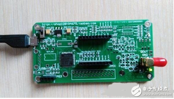
Figure 1 shows the control board. The right side of the board is the power interface using the mobile phone's standard Micro-USB interface, each mobile phone charger can be used as a power supply, the power supply is very convenient. Close to the Micro-USB interface is the power switch. On the left side of the board is the SAM RF output interface. The two black females in the middle of the board are the AD9850 modular jacks. The 4-pin female in the lower left corner of the board is the HC-06 Bluetooth serial port module socket.
Control panel size: 99.8*50.8MM, board thickness 1.2MM.
Installation hole distance: long distance 92MM, width 43MM. It is a 3.6MM through hole and can be fixed with 3MM bolts.
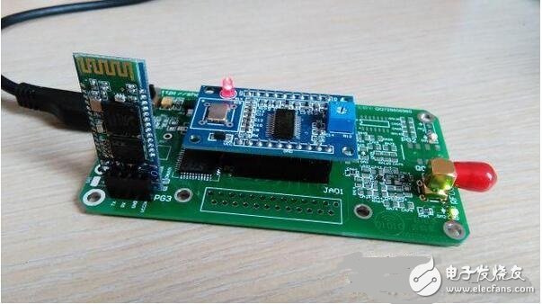
Figure 2 shows the combination of the AD9850 board, control board and Bluetooth serial board. Note that the VCC pin of the AD9850 module must correspond to the + power supply pin of the upper row of the control board. If the plug is reversed, the module will be damaged. Note that the VCC pin of the HC-06 must correspond to the VCCIN pin of the 4-pin female in the lower left corner of the control board. Tip: If you solder the pins of the Bluetooth serial module, rotate it 90 degrees and plug it into the control board. The height of the modular module is thus much reduced, and it can be housed in a small aluminum profile box.
The corresponding AD9850 pins are as shown below. Now they are all upgraded blue boards, and the pins are the same. The two rows of pins have a span of 20.5 mm and a pitch of 2.54 mm. A row of 10 pins, a total of 20 feet.
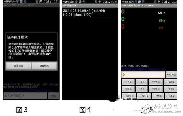
Figure 3 shows the selection interface of the Bluetooth serial port on the Android phone. Here, the keyboard mode is selected. Figure 4 shows the search for Bluetooth devices. The initial link pairing password is 1234. Figure 5 shows the socket interface after entering the keyboard mode. The upper part of Fig. 5 shows the output frequency of the current DDS module, the yellow shows the corresponding MHZ frequency, the green shows the corresponding KHZ frequency, and the red shows the corresponding HZ frequency. The user can enter the frequency you want in the input box at the bottom of Figure 5, and then press the send button to set the frequency. Below the input box is the commonly used frequency increase and decrease. Pressing a button will automatically generate the corresponding increase and decrease frequency.
Indicator introduction:1 Frequency range: 1HZ~40MHZ. The main clock of DDS is 125MHZ. According to Nyquist's theorem, the maximum frequency of 62.5MHZ can be generated, but the harmonics and distortion of frequencies above 40MHZ will increase.
2 frequency resolution: 1HZ
3 Output amplitude: -3.3dBm~-4.7 dBm. At 1MHZ, it corresponds to -3.3dBm, and 40MHZ corresponds to -4.7dBm.
STC15W4K48S4 microcontroller
AD9850 frequency synthesizer
An Android phone
Custom Wire Harness Assembly
- Electrified dimensional build boards with 100% continuity test
- Capabilities to test for fuse,diode,resistor, and relay presence
- Mating test fixtures for lower production wire harnesses
- Ability to free hand build harnesses for prototypes and design validation
- Separate layout boards for addition of fir tree clips, rosebuds, clamps,and labels after coverings added
- Capabilities to add board interlocks and test markings to harness as needed
Custom Wiring Harness,Wiring Harness,Cable Assemblies,Wire Harness,Wire Harness Assembly Manufacturer
ETOP WIREHARNESS LIMITED , https://www.oemmoldedcables.com