Organic light-emitting display diodes (OLEDs) have been increasingly used in high-performance displays as a current-type light-emitting device. Due to its self-illuminating properties, AMOLED has many advantages such as high contrast, ultra-thin, and flexible compared to LCD. However, brightness uniformity and afterimage remain the two main problems that it currently faces. To solve these two problems, in addition to the improvement of the process, the compensation technology has to be mentioned.
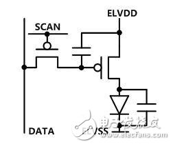
Before introducing compensation techniques, let's first look at why AMOLEDs need compensation. The figure below shows a simplest AMOLED pixel circuit that uses two thin film transistors (TFTs) to build a pixel circuit to provide the corresponding current to the OLED device.
Compared with general amorphous silicon thin film transistors (Amorphous-Si TFTs), LTPS TFTs and Oxide TFTs have higher mobility and more stable characteristics, and are more suitable for use in AMOLED displays. Low-temperature polysilicon thin film transistors (LTPS TFTs) are often used in small and medium-sized applications, and oxide thin film transistors (Oxide TFTs) are often used in large-size applications. This is because the LTPS TFT has a higher mobility and a smaller device footprint, which is more suitable for high PPI applications. The Oxide TFT has better uniformity and the process is compatible with a-Si, which is more suitable for producing large-size AMOLED panels on high-generation lines. Then they have their own shortcomings. Due to the limitations of the crystallization process, LTPSTFTs fabricated on large-area glass substrates often have non-uniformities in electrical parameters such as threshold voltage and mobility. Sex will translate into current and brightness differences in OLED display devices and is perceived by the human eye as the mura phenomenon. Oxide TFT has good uniformity of process, but similar to a-Si TFT, its threshold voltage will drift under long-term pressure and high temperature. Due to different display screens, the threshold drift of TFTs in different parts of the panel will be different. This causes a difference in display brightness. Since this difference is related to the previously displayed image, it is often presented as an afterimage phenomenon, which is commonly referred to as afterimage.
Therefore, in the current process of fabrication, both LTPS and Oxide have problems of uniformity or stability, and the OLED itself gradually decays with the increase of the lighting time. Since these problems are difficult to completely overcome in the process, they must be solved by various compensation techniques in design. Generally, the luminance of an OLED is proportional to the current, and the current is supplied by the TFT, which is related to the characteristic parameters of the TFT. The current is usually expressed as k is a parameter related to TFT mobility, and Vgs and Vds are in turn related to the power supply voltage and the OLED driving voltage. It can be seen that the parameters affecting the magnitude of the current include TFT mobility, threshold voltage, driving voltage of the OLED, and magnitude of the power supply voltage. The main purpose of the compensation technique is to eliminate the effects of these factors and ultimately achieve the desired brightness for all pixels. Because there are too many variables and the technology is very difficult, the compensation technology has become one of the core technologies of AMOLED display.
The compensation method can be divided into two categories: internal compensation and external compensation. Internal compensation refers to a method of compensating a sub-circuit built using TFTs inside a pixel. External compensation refers to the method of sensing the electrical or optical characteristics of a pixel through an external drive circuit or device and then compensating. Generally, the internal compensation pixel structure and driving method are complicated, and the compensation effect is limited to the TFT threshold voltage and IR Drop, and the compensation range is small, which is difficult to solve the afterimage problem. This type of compensation is not widely used in TV products, but it is also sufficient in applications where the frequency of use of mobile phones/tablets is not high and the product life cycle is short. The external compensation method has the advantages of simple pixel structure, fast driving speed and large compensation range, but the disadvantage is that the peripheral driving circuit has high design complexity. In large-size AMOLED TV display applications, external compensation is considered as a better compensation scheme. . However, recently, as users' requirements for product characteristics have increased, external compensation has gradually evolved into small and medium size applications.
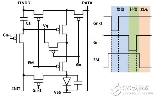
The following figure is a typical internal compensation type circuit, which consists of 7 TFTs and 1 storage capacitor. Therefore, it is abbreviated as 7T1C structure. Similar to many similar circuit structures such as 6T1C and 5T2C, it has been continuously researched in recent years. Development, the topology of the internal compensation circuit has almost been exhausted, and it is difficult to have practical structural innovation. This kind of pixel circuit generally has three working phases, which will undergo reset, compensation, and illumination. That is, a driving cycle must be at least 2 to 3 things, so there are certain requirements for the circuit driving capability and the load on the panel. Its general working idea is to store the threshold voltage Vth of the TFT in its gate-source voltage Vgs in the compensation stage. In the final illumination, Vgs-Vth is converted into current, because Vgs already contains Vth, which is converted into The current is offset by the effect of Vth, thereby achieving current consistency. However, due to the influence of parasitic parameters and driving speed, Vth cannot be completely canceled, that is, when the Vth deviation exceeds a certain range (usually Vth≥0.5V), the current consistency cannot be ensured, so its compensation range is said. It is limited.
External compensation can be divided into optical extraction and electrical extraction according to different data extraction methods. The optical extraction method refers to extracting the luminance signal by the method of optical CCD illumination after the backlight is illuminated, and the electrical extraction refers to extracting the electrical signals of the TFT and the OLED through the sensing circuit of the driving chip. The two methods extract different types of signals, so the data processing methods are different. The optical extraction method has the advantages of simple structure and flexible method, and thus is widely used at this stage.
The figure below is a schematic diagram of the external optical compensation. The OpTIcal sensor is usually a high resolution and high precision CCD camera.
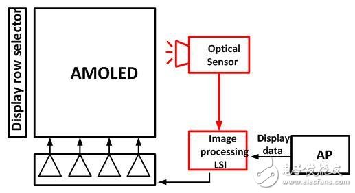
External optical compensation schematic
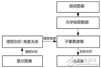
The compensation process is to take a picture of the entire panel with a CCD, obtain the brightness value of each pixel under several characteristic gray levels, and then model the sub-pixels to obtain the gray-to-luminance characteristic curve of each pixel. When compensating for a certain display image, we can deduct from the gray-light characteristic curve of the sub-pixel according to the ideal brightness corresponding to the input gray level, so as to make the sub-pixel reach the same brightness, the corresponding compensation Grayscale, for all sub-pixels to perform similar operations, we can get a so-called compensation image, using this compensation image to drive the backplane, we can achieve the desired brightness value. The difficulty of this technology is how to accurately capture the correct brightness of each pixel and establish a correct model with the CCD. It is necessary to overcome the problems of accurate positioning and moiré of sub-pixels through algorithms. Because optical compensation relies on specialized equipment, it can only be initialized and calibrated before leaving the factory, and it cannot be compensated in the use of the product. Therefore, it can only compensate for display non-uniformity and cannot compensate for the afterimage generated during use.
Optical external compensation scheme
Another way of external compensation is electrical compensation, that is, the IV characteristic of the driving tube and the IV characteristic of the OLED device are read to the external sensing circuit through the TFT inside the pixel, and the driving voltage value to be compensated is calculated and fed back to the chip of the driving panel. Thereby achieving compensation. It requires the development of new ICs with signal extraction capabilities.
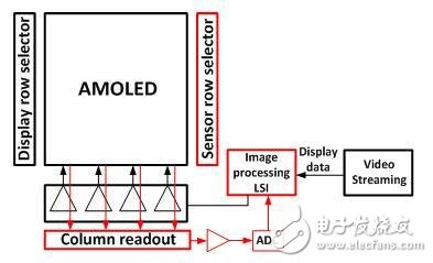
The role of Column readout in the figure is to monitor TFT IV characteristic variation and uniformity, monitor OLED uniformity and aging; Image processing LSI function is to calculate the compensation amount based on the monitoring result, and integrate the compensation amount and initial data into Data Driver.
The external compensation pixel circuit is relatively simple, usually the 3T1C structure is as shown below. In addition to the conventional data line, it has a sensing line (SENSE) that can extract the current of the TFT and OLED into the driver IC.
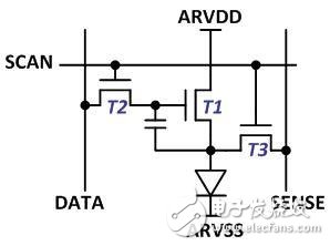
External compensation pixel structure
It has two ways to extract electrical signals, one is to extract TFT current, which is called TFT sensing, and the other is to extract OLED current, which is called OLED sensing. The basic principle is to give the driving voltage of the TFT or OLED, and draw the current from the sensing line to the driving IC, as shown in the figure below.
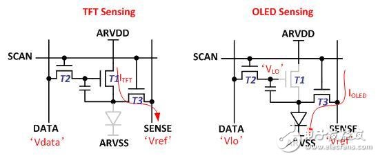
TFT and OLED sensing methods
After reading the electrical signal, the external compensation method can implement a more complicated algorithm by means of an external integrated circuit chip, and compensate for the non-uniformity of the threshold voltage and mobility of the TFT and the aging of the OLED. The technical difficulty of external electrical compensation is to realize high-precision and high-speed TFT&OLED electrical parameter reading. The parasitic effect on the sensing line will affect the reading speed and cause signal attenuation. The error of the sensing circuit will cause output distortion, adjacent sensing lines or the outside world. Environmental noise can interfere with the accuracy of the sensed signal. External compensation technology is a system-level solution that includes panel design, IC design, drive circuit design, and algorithm design. Any failure of any link may affect the compensation effect, but once accurate design is achieved, its compensation effect is the best. Real-time compensation can be realized, that is, continuous compensation during use during the product life cycle can effectively improve product life.
Because compensation technology is critical, many companies are actively developing compensation technologies with independent intellectual property rights. At present, the company with deep accumulation of internal compensation technology is Samsung. Only LG is the first in the external compensation industry to achieve mass production. Other panel manufacturers or companies are investing heavily in research and development for this technology. BOE has also developed internal compensation and external compensation technology with independent intellectual property rights, and has completed verification on the product side, leading in the country. . But even Samsung or LG, the current compensation technology can not be said to be flawless, but also need to continue to innovate and improve, along with the progress of the level of technology and capabilities, I believe that the future AMOLED products will be more perfect.
About the author: Wu Zhongyuan BOE VO SBU OLED development copy minister received a master's degree in microelectronics and solid physics from Tsinghua University in 2004, 2004-2010 in South Korea's Samsung Semiconductor engaged in display driver IC design, joined the BOE in 2010 has been focused on large-size OLED Technical field. Now responsible for large-size OLED technology and product development work. His main research interests include AMOLED pixel design, drive technology, compensation algorithms, and IC design. The main responsible 55 UHD AMOLED development, external compensation and other projects have won the Group Excellence & Excellence Project Award. He is currently a member of the Professional Technical Committee of SID Beijing Branch.
Ethernet Switches,Industrial Ethernet Switches,10 Port Ethernet Switch,5 Ports Ethernet Switch
Shenzhen Scodeno Technology Co.,Ltd , https://www.scodenonet.com