introduction
In recent years, software radio (SDR) has developed rapidly and has shown its superiority in many fields. The project background of this paper is the implementation of digital audio broadcasting (DAB) baseband signal processing by software radio, which requires the software radio platform to have high-speed real-time digital signal processing and transmission capabilities. High-speed programmable logic devices (FPGAs) and a rich IP core provide an ideal platform for efficient implementation of software-defined radio technology.
1 PCIE bus program demonstration
PCIE is the 3rd generation I/O bus interconnect technology and is now the leading standard interconnect bus for personal computers and industrial equipment. Compared to the traditional parallel PCI bus, PCIE uses a serial bus point-to-point connection for higher transmission rates and scalability. For example, the theoretical transmission rate of the 8-channel 1 generation PCIE 2.0 hard core used in this paper is 4 GB/s, and the bus width can also be selected according to the requirements of &TImes; 1, &TImes; 2, &TImes; 4 and &TImes; 8 channels. Compared to other serial interfaces such as RapidIO and Hypertransport, PCIE has better performance and greater flexibility.
1.1 PCIE bus implementation
At present, there are two main implementations of the PCI Express bus: a dedicated interface chip ASIC and an FPGA-based programmable logic device FPGA solution. The former usually adopts the combination of ASIC+FPGA/DSP. The dedicated PCIE interface chip (such as PEX8311) avoids the user's excessive contact with the PCIE protocol, which reduces the development difficulty; but the hardware circuit design is complex, the function is fixed, the flexibility and the scalability are Poor. The latter uses the IP core to implement the PCIE protocol, allowing users to develop the functions and drivers they need, with programmability and reconfigurability; in addition, the single-chip FPGA reduces cost and circuit complexity, and is more compatible with system-on-a-chip (SoC) Design ideas. This article uses Xilinx Virtex6 FPGA and PCIE integrated block to achieve high-speed PCIE interface design in double buffer mode.
1.2 Double buffering and single buffer comparison
Take the write operation (data from FPGA to memory) as an example. The block diagram of the double buffered PCIE system is shown in Figure 1. For convenience of description, the FPGA system on chip is named SRSE (Software Radio System with PCI Express).
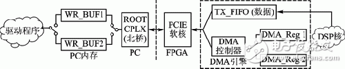
Figure 1 Double buffered PCIE system block diagram
The PC-side driver allocates two buffers (WR_BUF1/2) to the SRSE for data storage on the system memory. The address information of these two buffers is stored in the DMA register (DAM_Reg1/2) of the FPGA side. The Root Complex connects the CPU, memory, and PCIE devices. It represents the CPU to generate the transfer request. The PCIE core is an integrated block program provided by Xilinx, which implements the PCIE protocol. The DMA (Direct Memory Access) engine is used to implement the DSP core and the PCIE device. High-speed data storage and exchange; DSP (digital signal processing) core is a user-designed algorithm or application. Taking Figure 1 as an example, the DSP core writes the generated data to the TX_FIFO. The DMA engine sends the data to the PCIE core in the form of a Transport Layer Packet (TLP), where the header information of the packet comes from the register DMA_Reg1. When the SRSE writes the data When entering the buffer WR_BUF1, the driver allocates another buffer WR_BUF2 and writes the address information of the buffer to the register DMA_Reg2; when the DMA engine issues a write operation message interrupt (MSI) of WR_BUF1, the DMA controller will header the packet. The information is switched to DMA_Reg2, and the driver switches the buffer to WR_BUF2 to continue transferring data.
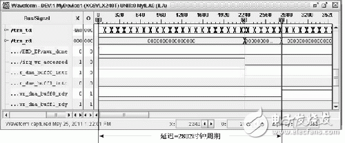
Figure 2 PCIE bus interrupt delay measurement
Corresponding to double buffering is the single buffer mode. Taking a write operation as an example, the driver allocates a buffer WR_BUF in memory each time, and the address information of the buffer is stored in the DMA register DMA_Reg. When the buffer WR_BUF is full, the DMA engine generates an MSI interrupt and notifies the driver through the PCIE core. The driver allocates a new buffer and writes the buffer address to the DMA register DMA_Reg via the PCIE bus. Interrupt transfers and DMA register updates generate a delay, which requires a larger TX_FIFO to access the data generated by the DSP core during the delay.
In order to accurately measure the interrupt delay time, a platform based on the DELL T3400 PC and ML605 development kit was built. The waveform results observed by ChipScope are shown in Figure 2. The DMA interrupt occurs at time 0 (mwr_done:0?>1); then the PCIE core issues an MSI interrupt to the driver, and the driver polls the interrupt register at time 2241 (irq_wr_accessed:1?>0); the driver allocates a new memory buffer. And then update the DMA register to occur at time 2802 (wr_dma_buff0_rdy:0?>1). During this 2802 clock cycles, the PCIE device was unable to write data to the memory. The clock frequency of PCIE is 250 MHz, so the interrupt delay is T=2802×(1/250 MHz)=11.2 μs. It is assumed that the data generated by the DSP core is 200 MB/s, and the interrupt delay period will be 11.2 μs×200 MB. /s=2241 B size data. Considering other unpredictable factors, such as interrupt blocking, the TX_FIFO requires at least a few kilobytes of space in order not to lose data. This is a serious challenge for valuable hardware resources such as Block RAM in FPGAs.
Compared with the single buffer mode, the advantages of the double buffer mode are summarized as follows:
1 Update buffers do not introduce interrupt latency, which means smaller FIFOs can meet demand and save hardware resources.
2 Double buffering mode extends the time the driver handles interrupts, and makes buffer data processing easier and packet loss rate greatly reduced.
3 Data transmission and data processing of the memory buffer can be processed in parallel, and the real-time performance of the system is guaranteed.
4 Double buffering is more suitable for Scatter/Gather DMA, replacing block DMA to improve memory efficiency.
2 Software radio platform design
Software radio is based on a programmable, reconfigurable, general-purpose hardware platform that implements different radio functions by loading different software and is widely used in military and civilian applications. In order to implement complex algorithms, its platform needs to have high-speed data exchange and real-time signal processing capabilities. The design is based on the Xilinx ML605 development kit, based on the Xilinx Virtex6 LX240T FPGA chip, and a common software radio platform is built by adding the appropriate modules.
The software radio block diagram is shown in Figure 3. The signal acquisition module uses two ADCs and DACs to realize digital-to-analog conversion of IQ two-way signals; the communication module is composed of Ethernet and USBRS232 interfaces; the expansion card can be an RF transmitter or receiver, and is connected to the motherboard through an expansion card interface; The JTAG interface provides in-circuit programming and internal test functions; the memory device includes 512 MB DDR3 memory and 128 MB platform Flash for dynamic data storage and configuration of FPGA; human-machine interface consists of LED/LCD, buttons and switches, etc. Machine dialogue; 200 MHz active crystal oscillator and SMA clock interface form a clock input module to provide clock reference to FPGA; 8-channel PCIE interface and IP core realize high-speed data exchange between platform and PC.
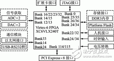
Figure 3 Software radio block diagram
The piezoelectric buzzers (for Driver Circuit Built-in) offer optimal sound, performance, and efficiency for all types of medical and industrial applications. Our piezo buzzers are constructed in a variety of sizes and work across varying frequencies which allows them to produce different sounds and tones. As voltage is applied to a Piezo Buzzer, the piezoceramic disc vibrates, flexing with respect to input voltage to generate sound. Our piezo buzzers maintain low current draw which is advantageous for any battery operated device. Since piezo buzzers don`t have a magnet in their construction, it eliminates EMI/EMC issues.
Piezoelectric Buzzer For Driver Circuit Built-in
Buzzer Alarm,Built In Piezoelectric Buzzer,High Frequency Alarm Buzzer,Constant Tone Buzzer For Alarm
Jiangsu Huawha Electronices Co.,Ltd , https://www.hnbuzzer.com