In a radio frequency receiver, radio frequency signals are transmitted through unit modules such as filters, low noise amplifiers, and intermediate frequency amplifiers. Since each unit has inherent noise, the output signal-to-noise ratio is degraded. With a multi-stage cascade system, the noise figures of the previous stages have the greatest impact on the system. In order to reduce the noise figure of the whole system, the noise coefficients of the first and second levels must be reduced and their power gains should be appropriately increased to reduce the influence of noise at the subsequent stages on the system [1]. The low noise amplifier LNA (L0W-Noise Amplifier) ​​is the key component of the front end of the radio frequency receiver. It requires: (1) minimum noise and a certain gain. (2) It is required to have a sufficiently large linear range. (3) It is required to have a good match with the input and output ports to achieve maximum power transfer or minimum noise figure, which are difficult to achieve at the same time, and a compromise is needed. (4) It is required to have a certain frequency selection function to suppress the interference of the out-of-band and image frequency. Based on the above four requirements of low noise amplifier, this paper discusses the design method of low noise amplifier from the aspects of noise optimization, impedance matching and small signal gain under power consumption limitation, and designs a working mode in 2.4 using 0.25μm CMOS process. Fully integrated low noise amplifier for GSM frequencies that can be applied to transceivers in Bluetooth systems.
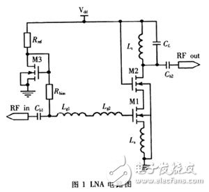
1 Circuit Analysis and DesignThe low noise amplifier (LNA) implemented by the basic circuit form [2-3] of the inductor source with negative feedback and single-ended input is shown in Figure 1. In the figure, M1, M2 and LS form an inductive negative feedback cascode casocode amplifier circuit to achieve high isolation, low noise figure and good input impedance matching. In the input loop, Lgs1, Lg2, and Cgs1 and Ls of M1. The resonance is at 2.4 GHz and matches the input 50 = Ω impedance. Cb1 is the DC blocking capacitor at the input. In the output loop, the equivalent capacitance of the drain of Lt and M2 resonates at 2.4 GHz. M3, Rref and Rbias form a bias circuit, and the size of Rref can be adjusted to control the DC operating point and static power consumption of the circuit. The bias voltage of the M1 gate is mainly determined by Rref and M3, and Rbias can be fine-tuned.
The main amplifier tube M1 contributes the most to the noise of the circuit, mainly as channel thermal noise and gate induced noise. According to the noise theory [4-5], the larger the channel width W and the quiescent current, the smaller the noise, but the actual design must consider the power consumption limitation, and it is impossible to reduce the noise by increasing the power consumption. The power consumption requirement of this design is less than 15mW. The following is used as a constraint to derive how to choose the size of M1 to obtain the optimal noise.
The approximate expression of the system noise figure is:
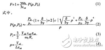
Where γ and δ are the MOS tube channel thermal noise coefficient and the induced gate noise figure, respectively, c is the correlation coefficient between the two kinds of noise (the values ​​of which are determined by the process), ω0 is the resonant frequency, υsat, εsat Respectively indicate the saturation speed of the electron and the electric field strength at which the speed is saturated. Rs is the 50 Ω source impedance, PD is the circuit power consumption, Po is the output power, Vdd is the supply voltage, and Vod is the output voltage.
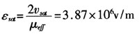
0.25μm CMOS RF by Charter. The process can determine the minimum channel length L≌0.241μm, the electron saturation velocity υsat=76090m/s, the effective mobility of electrons μeff=0.03932m2/(υs), and the speed saturation electric field strength is
The noise figure F has the following close relationship with the M1 size selection:
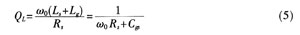
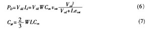
In the formula, QL is the quality factor of the input resonant resonance, Cgs is the capacitance between the MOS tube gate source, and Cpx is the capacitance density of the MOS gate oxide layer. Available from equations (3), (4), (5), (6), (7):
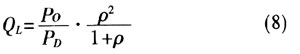
For each power consumption value, it corresponds to an optimal Ql, opt value, so that the noise figure under the power consumption is minimized. Using Matlab mathematical software analysis, QL is obtained when the minimum noise is obtained under the power consumption limit of 15mW, and opt is 9.2. The generation of the following formula can calculate the channel width of M1 as:
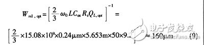
In this design, the channel width and length of M2 are the same as M1, and are also taken as Wm2≌160μm, L≌0.24μm.
1.2 impedance matching [6]The input impedance of the low noise amplifier can be written as:
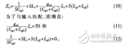

The 60W Macbook Charger with MagSafe1 or Magsafe 2 Power Adapter has a magnetic DC connector, so if someone trips on it, the power cord disconnects harmlessly, keeping your MacBook Air safe. It also helps prevent the cable from fraying or weakening over time. Additionally, the magnetic DC helps guide the plug into the system for a quick and safe connection.
60W Apple charger usb c,60w charger macbook air,macbook 60w charger
Shenzhen Waweis Technology Co., Ltd. , https://www.waweispowerasdapter.com