Tag: AC/DC Converters Photocouplers
This article refers to the address: http://
With the continuous advancement of semiconductor technology, it provides an advanced technology platform for system designers and circuit designers to realize technological innovation, so that many novel and fashionable portable electronic products are presented to the world, such as PDA and 3G mobile phones. , a variety of personal electronic health care devices and endless game consoles and so on. Most of these portable electronic products require high-end switching power supplies for powering or charging. In addition, there are many advanced portable instrumentation, industrial control devices and even everyday appliances such as razors that require switching power supplies. It is against this background that PHILIPS has launched the STARplug power IC product line.
This series not only meets the requirements of micro power consumption, high reliability, and miniaturization of portable electronic products, but also meets the requirements of safety and environmental protection.
About the STARplug product line
STARplug has two series, TEA152X series and TEA162X series (see Table 1). The TEA152X series was introduced as early as September 2000. The TEA162X series is an improvement of the TEA152X series, which was finalized in May 2004. The two are in block diagram, circuit structure, external lead arrangement and most electrical parameters. Are the same. The difference is only in the internal high-voltage starting current source of the chip, TEA152X series Icharge=1.5mA (typical), TEA162X series Icharge=500uA (typical).
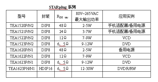
Note: Table 1 only lists the dual in-line package, and the surface is not listed.
STARplug uses a multi-chip architecture. All control sections are integrated on one chip using a BiCMOS process, while the power section is fabricated on another chip using the EZ-HV process and then optimized on the same substrate. From the manufacturing process point of view, Philips uses an advanced full oxidation isolation process (or media isolation process), so it has the following characteristics:
1. The lock-in effect can be dispensed with (the lock-in effect is a failure mode unique to CMOS circuits);
2. It is easy to integrate analog, digital and power circuits on the same chip;
3. The chip area is also smaller than the standard PN junction isolation;
4. Leakage current is extremely low, suitable for working in high temperature environment;
5. The parasitic capacitance is small, and the probability of crosstalk and EMC generated through the substrate is small;
6. Strong ability to resist external sparks and reverse polarity.
These are all beneficial to support the high performance and reliability of STARplug.
From the perspective of circuit design, an important feature is the concept of valley conversion.
In general, the power dissipated by the power MOSFET is the main source of power consumption of the switching power supply. It is closely related to the reliability, stability and efficiency of the power supply. The power consumption of a power MOSFET is usually composed of three parts:
1. The power consumption when the MOS transistor is turned off, that is, the power consumption of VDS is high: This power consumption is mainly determined by the leakage current between the drain D and the source S, which is related to the chip manufacturing process, IDS(off) Usually in the order of micro-amps, so this part of the power consumption is extremely low, generally negligible.
2. The power consumption when the MOS transistor is turned on, that is, the power consumption when VDS is low. This power consumption is mainly determined by the on-resistance RDS(on) between the drain and the source. This is related to the geometric parameters of the chip design.
3. MOS tube dynamic power consumption, that is, the MOS tube is switched by the cut-off conduction, or the power consumption from the turn-on to turn-off conversion. This power consumption can be calculated by:
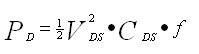
Philips' circuit designers analyzed the above formula and realized that to reduce the dynamic power consumption of the switching power supply, it can only be achieved by reducing the VDS during conversion and the f when the load drops. Usually, the VDS is about 380V. If the VDS is turned to the bottom (close to 0V) by circuit resonance, the dynamic power consumption of the MOS transistor will be reduced by several orders of magnitude. For this reason, in the circuit design, a valley detection circuit is added, and once the circuit is resonated, the "valley" can be correctly measured, and when the VDS enters the "valley", the input between the gate G and the source S is input. The rising edge of the pulse after PWM.
In the PWM chips of the 1990s, the operating frequency f was mostly a fixed frequency. In order to reduce power consumption, especially to reduce standby power, STARplug has adopted a flexible circuit design with adjustable frequency. The frequency set by the user is the operating frequency at full load. When the load drops, the operating frequency also drops accordingly. This ensures that the standby power consumption is less than 100mW.
In addition, the STARplug series of chips are started with a high-voltage current source. Once the IC enters normal operation, the high-voltage current source will be automatically cut off, thus reducing the power consumption of the circuit. This shows the entire design process of the circuit. The idea of ​​reducing power consumption has been implemented. It is precisely because the power MOSFET and the control part effectively reduce power consumption significantly, so that the power device and the control circuit can be integrated in one package, which effectively reduces Peripheral components. In addition, in order to make the circuit work reliably, it also provides perfect protection functions, including cycle-by-cycle overcurrent protection, undervoltage lockout, overvoltage protection, overtemperature protection, winding short circuit protection, and demagnetization protection.
STARplug function description
1. Structure of STARplug
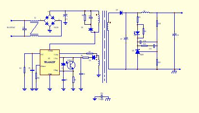
Figure 1 is a block diagram of the internal circuit of STARplug. It is not difficult to see that the figure includes two parts of the power MOS tube and the control circuit. The power MOS transistor is mainly used to realize power transmission and conversion. The control circuit has three major tasks:
1. Achieve rapid response to all protection functions.
2. Accurate detection of valley levels.
3. Control of the duty cycle (ie PWM function).
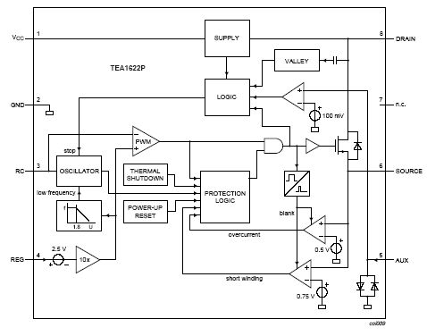
Figure 1: STARplug internal circuit block diagram
STARplug is based on a discontinuous mode (DCM) flyback topology. There are two ways to feedback:
1. Transformer auxiliary winding feedback, (this winding is also used as the power supply for the IC) (see Figure 2).
2. Transformer secondary winding via optocoupler feedback (see Figure 3)
2. The working principle of STARplug (see Figure 1, Figure 2).
After the AC power supply is rectified and filtered, it outputs Vdc, and is added to the DRAIN terminal of TEA162X through the transformer primary (8th pin, abbreviated as Dr). The high-voltage current source inside the chip (Fig. 1) passes through the Vcc terminal (1st pin) to the capacitor. C5 is charged. When the C5 charging voltage Vc5 reaches and exceeds the lower limit of 9V of the VCC starting voltage, the TEA162X starts to work.
As the first work of the TEA162X, power-on and clear (see Figure 1), the logic circuit in the chip is in the initial state, and the MOS power transistor is at a low level. The primary inductance of the transformer has a current through it and gradually increases. At the same time, the resistor R and capacitor C connected to the RC pin cause the oscillator to oscillate. The PWM comparator and driver convert the MOS power transistor from low to high. The energy stored in the primary inductance and the core air gap is then immediately transferred to the secondary and auxiliary windings of the transformer. The alternating voltage induced by the auxiliary winding is rectified and applied to the VCC terminal. When this voltage reaches the VCC starting voltage, the current sent by the high voltage current source interrupts it and is replaced by Vaux, so that the TEA162X continues to operate. Once Vaux falls below the Vcc start level or enters the stop level, the TEA 162X stops switching and is restarted by the rectified grid voltage Vdc.
STARplug is a voltage-controlled PWM circuit that controls the primary peak current through the transformer by modulating the on-time of the internal power MOS transistor of the chip to stabilize the output voltage.
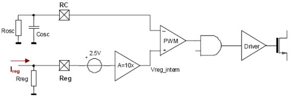
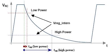
To illustrate the STARplug voltage regulation mechanism, the relevant parts of the TEA162X series of practical circuits are described as Figures 4 and 5. It is easy to see from the figure that the two inputs of the PWM comparator, one is the RC terminal (the third leg) and the resistor Ross and the capacitor Cosc are used to set the switching frequency of the circuit. The other is the external voltage connected to the Reg terminal (pin 4), which reflects the change in output load. The difference between the voltage applied to the Reg terminal and the internal voltage source of the chip (2.5V) is multiplied by 10 times, which is the signal voltage Vreg-intern applied to the PWM terminal. Vreg-intern and VRC are compared on the PWM comparator. If VRC is lower than Vreg-intern, the PWM output is "1" level and the power MOSFET is turned off. If the Vreg-intern is higher, the shorter the MOS tube conduction time, the smaller the power of the MOS tube conversion. Conversely, if Vreg-intern is lower, the longer the MOS tube is turned on, the greater the power converted. (See Figure 5)
3. Circuit protection function
In order to clarify the protection function of the circuit, we will draw the relevant parts inside and outside the chip separately as Figure 6. Source is the 6th pin of STARplug, externally connected with a resistor Rsrc to ground, and its resistance is determined according to the threshold of overcurrent protection.
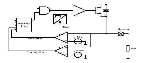
Figure 6: STARplug Protection Circuit Diagram
It is apparent from Fig. 6 that the current flowing through the power MOS transistor is converted into a voltage via the resistor Rsrc, and is applied to the non-inverting input terminals of the two comparators inside the chip, so that STARplug realizes overcurrent protection and output short circuit protection, respectively.
Overcurrent protection
When the load is increased or other causes the instantaneous voltage measured in a single cycle on the Source leg is greater than 0.5V of the voltage source inside the chip. Then, the output of the comparator will turn off the power MOS transistor, thereby cutting off the operation of the large current and protecting the power MOS tube.
To prevent false overcurrent signals from being detected, a disable is added to the comparator. The comparator operates when the overcurrent signal exceeds 350 ns.
Output short circuit protection
For some reason, shorting the output or shorting the winding causes the voltage on the Source leg to rise rapidly, so that it exceeds 0.75V. The other comparator will stop the conversion and the MOS transistor will be turned off, preventing the current from continuing to increase. The same comparator also takes the same measures to prevent false signals.
STARplug also provides precise over temperature protection. When the junction temperature exceeds the thermal shutdown temperature (typically 160 °C), the circuit will stop operating and the supply current will drop below the startup current. Once the junction temperature drops below the turn-off value, the circuit will resume operation.
Demagnetization detection
STARplug is always working in discontinuous conduction mode (DCM).
As can be seen from Figure 7, the auxiliary winding of the transformer is connected to the Aux leg of the circuit through a resistor. The chip has two reverse-connected diodes inside to clamp the input voltage. As long as the secondary diode is conducting, the voltage of the auxiliary winding is positive and current is injected into the Aux terminal and clamped by the diode. As long as the voltage at the Aux terminal is greater than 100mV, the oscillator stops working and the MOS transistor cannot be switched.
In the degaussing time tsuppr (typically 15 us), it is confirmed that the residual magnetism has been eliminated. This feature is especially useful for applications where the output voltage is low and the leakage inductance of the transformer is large.
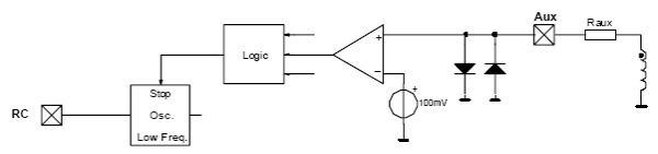
Figure 7: STARplug Demagnetization Detection
Overvoltage protection
In the block diagram of the chip, although there is no dedicated channel for overvoltage protection, this function exists. In the actual application process, once an overvoltage is generated, the operating level of the REG terminal is necessarily pulled up, so that the working stroke of the primary winding is immediately terminated. Only when the overvoltage is removed, the voltage of the REG terminal returns to the normal value, and the power MOS transistor can be normally switched.
STARplug application
As mentioned above, STARplug has two feedback methods, which constitute two typical application circuits of STARplug as flyback AC/DC converter.
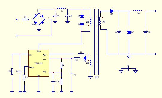
Figure 2 is the simplest and most basic application circuit, characterized by feedback from the auxiliary winding of the transformer to the changes in the grid and load.
As can be seen from Figure 2, the input portion of the circuit is composed of a rectifier bridge and a filter, and is applied to the Drn terminal of the TEA 162x through the primary winding of the transformer. Obviously, the TEA162x is the heart of the entire converter. The following sections of the circuit of Figure 2 are analyzed around the TEA162x.
1. The oscillation circuit is composed of C3R2.
The value of the oscillating circuit component is determined according to the operating frequency. The switching frequency of STARplug can work between 10kHZ and 200kHZ. Generally, the operating frequency is selected between 40~100kHZ.
When the frequency is selected, the component value can be calculated as follows:
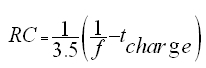
The charging time tcharge of the oscillator is found as 1us in the STARplug parameter table.
As for the value of RC, you can first select C and then calculate the R value. To keep the circuit stable, the capacitance C must be greater than 220pF. However, considering the efficiency, it is not appropriate to select the capacitor too much when the frequency is high. At 200kHZ, C takes 10nF, and the power consumption of the oscillator reaches 12.5mW, which is obviously not desirable.
Recommended example: The switching frequency is 100kHZ. At this time, the oscillator has a time constant of 2.7us, C takes 330pF, and R=7.5kΩ.
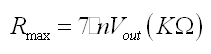
2. Overcurrent protection and winding short circuit protection resistor R3:
Resistor R3 sets the primary peak current of the transformer and also sets the output power of the maximum transmission. The value of resistor R3 can be calculated by:
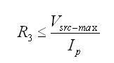
According to the manual of the STAR plug:
Example: A 3W power supply with a switching frequency of 100kHZ and an efficiency of 75%. The peak current through the transformer is 230mA (reflected voltage), then the resistor R3 is set to 2Ω and the peak current is limited to 250mA.
3. Regulator components R4 and R8:
In the circuit of the auxiliary winding feedback, the output voltage is controlled by the auxiliary winding. In fact, all windings in the transformer have the same flux variable, and the secondary output voltage and the auxiliary voltage VCC are related by the transformer turns ratio Na/Ns. The voltage information of VCC is again supplied to the REG terminal through a resistor divider, that is, R4 and R8. Therefore, the TEA162X directly stabilizes the output voltage of VCC and indirectly stabilizes the output voltage.
The values ​​of these two resistors can be determined by:
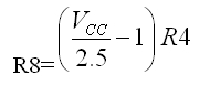
To prevent the effects of transient high voltage on REG, it is recommended that the value of R4 be between 3k and 10kΩ.
4, demagnetization resistance R5:
This resistor is used to limit the current flowing into the Aux leg. According to the technical conditions of the product, the maximum current flowing into the Aux leg is 5 mA, and the maximum current flowing out is 10 mA. Based on this, the product designer gives an approximate estimate. formula:
This formula should not be considered from the dimension, but only as an empirical estimation method.
5. Power supply circuit C5, R6, D8:
As mentioned above, the high-voltage starting current source in the chip charges the capacitor C5. When the charging voltage reaches the circuit starting voltage of 9V or more, the TEA162x operates. The value of C5 should be 1uF smaller, and 470nF is actually used in all applications.
The diode connected to the auxiliary winding only needs to use a common diode. The resistor R6 connected to the diode is used to prevent the instantaneous peak voltage. The resistance is determined experimentally. It can be selected between 56 and 560 Ω at the beginning of the experiment.
Figure 3 is a typical application circuit with feedback from a photocoupler. From the primary side, the biggest difference is that in Figure 3, the phototransistor is used to replace the resistor R8 in Figure 2, while the secondary in Figure 3 adds the LED and its sampling and driving circuit.
The AC/DC converter shown in Figure 2 is suitable as a voltage source, and its voltage regulation accuracy is related to the coupling degree of each coil of the transformer, which is about 8% or less, for those occasions where the stability is not high and the cost is high. , this option can be used.
If users with high requirements for voltage regulation accuracy and other parameters, such as users with a stable accuracy requirement of about 1%, the scheme shown in Figure 3 should be used.
Aluminum Die Casting,Aluminum Die Casting Parts,Aluminium Die Casting Process,Aluminium Die Casting
Dongguan Formal Precision Metal Parts Co,. Ltd , https://www.formalmetal.com