Transistor is also called Bipolar Junction Transistor (BJT). It is a current-controlled current semiconductor device with current amplification. Its main function is to amplify the weak input signal into an electrical signal with a large amplitude. The core components of commonly used electronic circuits.
There are two main symbols of the transistor, as shown in the following figure:

Among them, Q1 is an NPN tube and Q2 is a PNP tube. The direction of the E-pole arrow represents the actual direction of the current when the emitter junction is forward-biased. Their corresponding basic structures are as follows:

The basic structure of the triode is formed by stacking three mutually adjacent impurity semiconductors. Each of the three impurity semiconductor regions leads to one electrode. We call them Emitters and Collectors, respectively. Base, and the corresponding areas are called the emitter, collector, and base respectively. Two different types of impurity semiconductors adjacent to each other will form a PN junction. We set the PN between the emitter and the base. The junction is called an emitter junction, and the pn junction between the base and the collector is called a collector junction.
Transistors may have four working states (ie, amplification, cutoff, saturation, and inversion) in practical applications. Here we take the NPN triode as an example to explain in detail the working principle of the triode amplification state (PNP is similar, this article will not repeat them):
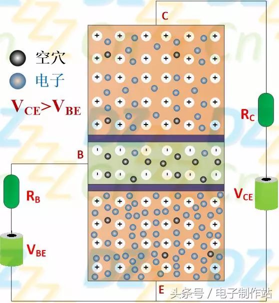
As the saying goes, the world is in a big trend. It must be a long time. It must be a long time. In this small area made up of three semiconductors, a history of the Three Kingdoms of the Central Plains is also staged. Our story takes place in this area as shown in the figure below. :

The first goal: In this seemingly peaceful era, there are always surging forces that are lurking. As soon as the time is right, the war will be triggered. The base area is a small country, and it is also a common neighbor of the collector area and the launch area. The country, in order to survive in this crack-down era, the base area is always developing its own dark forces (sub-teaching) in the collector area and the launch area!
The NPN transistor comprises a P-type semiconductor (base region) sandwiched by two N-type semiconductors (emission region and collector region), wherein the base region is thin and the doping concentration is low (so the majority carrier holes are also few, and a few There are even fewer carrier electrons, and the weak country!) The emitter and collector regions are both N-type impurity semiconductors, but the doping concentration of the emitter region is much higher, the troops are stronger, and the collector area is larger than the emitter region. Large area, a vast territory.
The second goal: Dawn just dawned, a million-strong army set out from the base of the launch area, and swept its way to the northern base-shot border. The commander of the launch area received an order: The aim of this round of dispatch was to level out the northern marginal tribes. (especially the collector area), making it subject to rule! This plan has been set up for a long time, but it has not waited until the spies reported recently: the Shoucheng coach of the collector area ordered the deep trenches in the city to strengthen the defense! The opportunity has come.
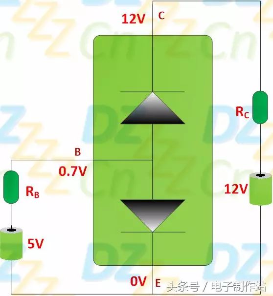
Two NPN voltages were originally applied to the NPN transistor, which had not been treated before, as shown in the following figure:
To make the NPN tube in amplifying state, the voltage VCE applied across the CE junction is greater than the voltage VBE applied to the BE junction. Therefore, the potentials of the three poles of the NPN tube are: VC>VB>VE, (the emitter potential VE is the reference potential 0V). In this way, the emitter junction of the transistor is forward biased, and the collector junction is reverse biased, which is the basic condition for the transistor to be in an amplified state.
(At the instant of voltage connection) Assume that the base-emitter (emitter junction) bias voltage VBE=5V and the collector-emitter bias voltage VCE=15V, two N-type semiconductors and P-type semiconductors form two PN junctions The BE junction (emitter junction) is forward biased and turned on to limit the base potential to 0.7V (silicon tube), while the collector potential is 15V due to reverse bias bias of the PN junction (instantaneous potential, at this time Electrode current is not yet there, as shown below:
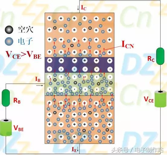
Well, everything is ready. A war is about to begin. Let's take a look at the flow of internal carriers in the triode (major carriers and minority carriers must be observed at the same time).
The third goal: The base area is a small country. No matter what aspects it can not compare with the big country in the launch area, we can see that the millions of troops are not evasive. After a little resistance, we have made a wise idea. Incomparable decision: open the gate to surrender! Soon, the troops in the launch area crossed the base-shot border.
When the emitter junction is applied with forward voltage VBE (forward bias), the doping concentration in the emitter region is high (the highest of the three regions), while the doping concentration in the base region is the lowest, and the majority carrier electrons in the emitter region. A constant diffusion of ions through the emitter junction to the base region (as already mentioned in the article "Diodes": transfer of carriers from a high concentration region to a low concentration region due to a concentration difference, called diffusion) forms emission Junction electron diffusion current IEN (the direction of the current is opposite to the direction of electron motion);
At the same time, the majority of carrier holes in the base region also diffuse to the emitter region, forming a hole diffusion current IEP (the current direction is the same as IEN). Obviously, the IEP is small compared to IEN, however, the revolutionary The power is of any size. We must unite all the forces that can be united before we can finally... I'm sorry to say that!
Adding both IEN and IEP is the emitter current IE, as shown in the following figure:

The fourth goal: The million-strong army has successfully captured the base city. It is in full swing. Because the base area has not had much resistance, the percentage of troops in the launch area has basically not been damaged. As the saying goes, “there is a bangâ€, therefore, the coach ordered the army to continue northward. However, No one would have thought that there were a small number of people in the million-strong army who took the opportunity to liaise with and deploy to the base.
The majority carrier electrons diffused from the emitter region to the base region have the highest concentration near the base-shot boundary (emitter junction), and the farther away from the emitter junction (northward) the lower the concentration, resulting in a certain electron concentration difference. The difference causes the electrons diffused in the base region to continue to spread in the direction of the collector junction (northwards).
In the process of electron diffusion, a small portion of electrons recombine with the majority carrier holes of the base region, thereby forming a base current IBN. We have already said in the foregoing that the base region is very thin and has a low doping concentration. Therefore, there is less chance of electron and hole recombination, and the base current IBN is also very small. Most of the electrons will be diffused to the set-base boundary (collector junction). ),As shown below:

The fifth item: As the spies return, the collector area had known that the launch area had the intention of attacking the country. It had already told us to continue to widen and reinforce all the cities to prevent all possible attacks. However, the launch area coach has long been prepared: Since you want to ditch the high base and avoid the war, I will let you "be successful, defeated Sri Lanka," and use the spear to attack the shield. Ever since, the army has made food more and more, starting in five.
Since the collector junction is a reverse bias voltage, the internal electric field in the space charge region is further strengthened (the PN junction becomes wider), which in turn has a strong attraction to the carrier electrons that diffuse into the collector junction at the base region ( The electrons are negatively charged and the same sex is attracted to the opposite sex, causing them to quickly drift past the collector junction (as mentioned in our article “diodeâ€: the carrier movement caused by the attraction or repulsion of an electric field is called drift). The collector current ICN is formed (the direction is opposite to the electron drift direction).
Obviously, ICN=IEN-IBN, because a small portion of millions of troops is in the base area, and the rest is in the collector area, as shown in the following figure:
Someone asked: The carrier electrons in the launch area all went to the base area and the collector area. Will there be no electrons afterwards? Hey, there are power supply VBE and VCE outside, and it can provide more continuous electronics.
Sixth head: Thanks to the wonderful plan of the head coach of the launch area, the launch area troops successfully captured the catchment area and formed a uniform pattern throughout the area, but the remnants of the catchment area also took the opportunity to mix into the base area or launch. In the district, crouching on standby, they may run out at any time to undermine national unity.
After the majority of carrier electrons enter the collector region, the minority carrier holes in the collector region (N-type) and the minority carrier electrons in the base region (P-type) also generate drifting motion, forming a current ICBO. , and some will cross the base area to reach the launch area to form the ICEO, as shown below:
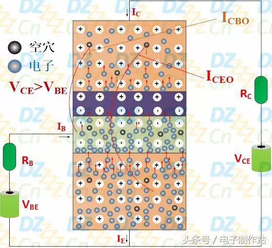
ICBO represents the collector-base reverse saturation current, ICEO represents the collector-emitter reverse saturation current (also collectively referred to as the penetration current), they are not controlled by the emitter junction voltage VBE, nor do they contribute to current amplification. It depends only on the temperature and the concentration of minority carriers, of course, the smaller the better. Under the same conditions, the penetration current of the silicon tube is smaller than that of the neodymium tube. In some high-power applications, an external current release resistor must be connected to prevent the triode from overheating and damage due to the penetration current. Duncan")
Item 7: The facts are: In view of their inherent circumstances, the base area has been developing dark forces in the launch area and the collector area. This war is an indirect measure. It uses the decision-making layer of the launch area to make the launch area coach send troops (collector area The intelligence of the deep trenches is transmitted by the base area. The troops in the launch area are used to destroy the collector area. That is to say, the initiative is still in the hands of the base area. As long as the pressure on the launch area is controlled, the launch can be launched. District power for their own use! A good trick "to catch crickets, yellow tits in the post"
In the transistor's amplification state, as long as the voltage of the emitter junction VBE is controlled, the base current IB will change accordingly, and then the majority of the current-carrying electrons in the emitter region will be controlled, and eventually the collector current IC will also be controlled.

From the principle of transistor amplification, it can be seen that the so-called "amplification" is not to amplify the base current IB, but is to use a smaller base current IB value to control the larger collector current IC value from the external circuit It looks like IB is being amplified, and this is also a reason with the "twinning".
Our factory can produce the galvanized steel poles with various heights.
Steel Lighting Pole,Steel Lamp Post,Metal Lamp Post,Metal Pole For Outdoor Lights
Jiangsu Baojuhe Science and Technology Co.,Ltd. , https://www.galvanizedsteelpole.com