From the perspective of electromagnetic compatibility, we need to pay attention to the following four types of wiring: A strong radiation signal line (high frequency, high speed, clock trace is represented) B sensitive signal (such as reset signal) C Power Supply signal D interface signal (simulation Interface or digital communication interface)
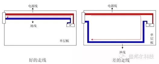
First, single and double-sided wiring design1. In a single-layer board, there must be a ground line near the power supply line and its parallel and parallel lines. Reduce the power supply loop area and reduce differential mode loop radiation.
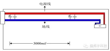
2. Power supply single-panel or double-panel, Power Cable trace is very long, add decoupling capacitor (10uF +1000pF) to ground every 3000mil. Filter out high frequency noise on the power line.
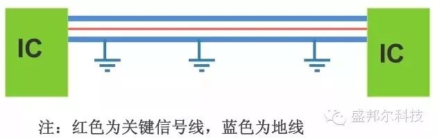
3.Guide Ground Line For single and double board, “Guide GroundLine†should be placed on both sides of the key signal line. The “clad ground†on both sides of the critical signal line reduces the signal loop area on the one hand and prevents crosstalk between the signal and other signal lines.
4. The reflow design is in single-layer or double-layer boards. When designing, attention should be paid to “minimum reflow areaâ€. The smaller the loop area, the smaller the external radiation of the loop and the stronger the interference.
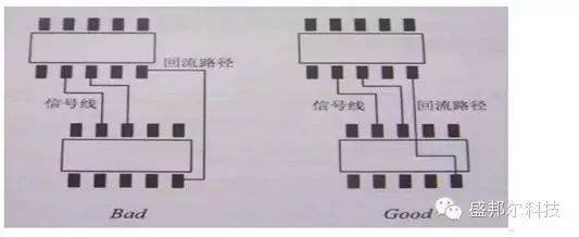
For multi-layer boards, the critical signal lines are required to have a complete signal reflow, and finally the GND plane reflow. The second most important signal is a full planar reflow. Signal crosstalk is prevented by reducing the loop while reducing external emissions.
5. Right-angle routing PCB traces must not have right-angled traces. Right-angled traces cause impedance discontinuities, causing signal emissions, which can cause ringing or overshoot, creating strong EMI emissions.

6. PCB trace thickness should be consistent. When the thickness is inconsistent, the impedance of the trace is abrupt, causing signal reflection, resulting in ringing or overshoot, resulting in strong EMI radiation.

7. Adjacent wiring layers Note that in layered design, the wiring layers should be avoided. If it is unavoidable, the parallel signal traces on the two wiring layers should be properly extended to cause signal crosstalk. The layer spacing between the line layers reduces the layer spacing between the wiring layer and its signal loop, and the wiring layer 1 and the wiring layer 2 are not adjacent.
Adjacent cloths should avoid the layer arrangement of adjacent wiring layers as much as possible. When it is unavoidable, the traces in the two wiring layers should be perpendicular or parallel to each other with a length of less than 1000 mils, thus reducing the crosstalk between the parallel traces.

The differential signal lines should be in the same layer, equal length, and walking line, and the impedance should be consistent. There is no other trace between the differential lines. This ensures that the common mode impedance of the differential pair is equal, improving its anti-interference ability.
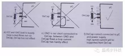
8. For the surface-mount fuses, beads, inductors, and tantalum capacitors used for power supplies with a via-effect current ≥1A, no less than two vias should be connected to the planar layer. The main purpose is to reduce the equivalent impedance of the via.
9. The grounding wire and the connecting power Cable of the capacitor wiring filter capacitor should be as thick and short as possible. The equivalent series inductance will reduce the resonant frequency of the capacitor and weaken its high-frequency filtering effect. There are also certain requirements for the grounding wire and the power cable routing between the filter capacitor and the chip pin.
10. Cross-segment design key signal traces must not be routed across the partition (including vias and pad-referenced reference plane gaps); routing across the partitions results in an increase in signal loop area. The solution is to increase the bridge capacitance or improve the partition.
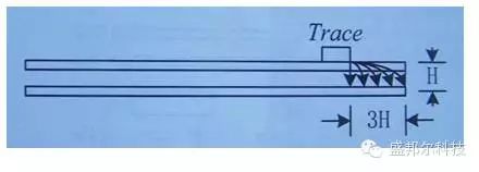
1. 3H principle For critical signal lines such as clocks and high-speed addresses, the reference plane edge is ≥3H (H is the height of the line from the reference plane), which can suppress the edge radiation effect well.
2. High frequency signal routing
In the multi-layer board, whether the TOP and BOTTOM layers of the single board have no signal line ≥50MHz, it is better to walk the high-frequency signal between the two plane layers, and the key signal can be shielded in the internal routing layer. To suppress its radiation to the space.

3. High-speed cable package
It is recommended to cover the grounding line on both sides of the clock. The grounding line is grounded every 3000 mils to ensure that the potentials at the points on the grounding line are equal. Key signal traces such as CLK, BUS, and RF lines and other parallel traces in the same layer should meet the 3W principle. The same is true between layered traces to avoid crosstalk between signals.

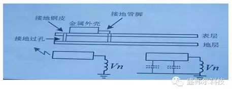
4. The metal case needs to be grounded. For the metal case, the grounding element (such as crystal, heat sink case, and reinforced metal frame) should be grounded. The copper film should be grounded on the top layer of the projection area, and the distributed capacitance between the metal case and the ground copper pad should be To suppress its external radiation and improve the immunity.
1. Strong radiation trace clock line, bus, RF line and other strong radiation signals away from the interface outgoing signal line, to avoid interference on the strong radiation signal line coupled to the outgoing signal line, radiating outward.
2. Strong sensitive trace signal lines such as reset signal lines, chip select signal lines, system control signal lines, etc. are far away from the interface outgoing signal lines. Interface outgoing signal lines often introduce external interference, which can cause system misoperation when coupled to sensitive signals.
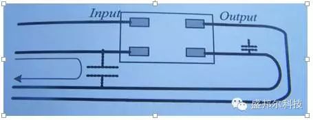
3. The input and output signal lines of the filter before and after the filter (filter circuit) cannot be parallel to each other and cross-routed. It is necessary to avoid direct noise coupling before and after filtering.
4. The connection between the function modules is as shown in the figure. If there is no interconnection signal line between the modules on the board, the modules are connected through the ground;
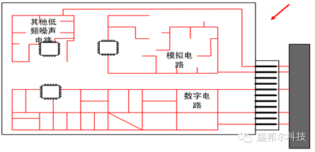
If there is a signal interconnection, the signal lines are connected at a single point across the module circuit. (Red is the ground network, blue is the signal interconnection, black is the ground connection between the networks)

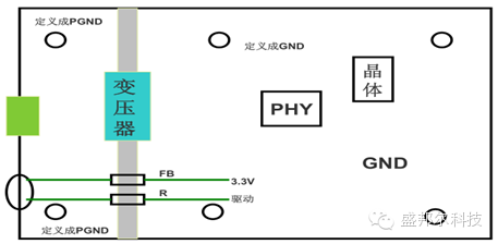
4. Example network interface wiring rules
1 All the underside of the transformer is hollowed out; 2 The width of the grounding slot is greater than 100 mil; 3 The distance between the connector and the isolation transformer is less than 1000 mil; 4 The distance between the crystal and the transformer is at least 1000 mil; 5 The lamp drives the current limiting resistor and the magnetic on the power supply The beads are placed in the hollowed out position.
5. Design points for grounding at the interface
1 The board interface grounds the metal structure of the device to make it “cleanâ€, which is used to ground the filter circuit and the protection circuit; 2 the ground of the power filter is connected to the board interface; 3 the power supply area of ​​the power module output Single-point digital ground; 4 digital interface circuit is recommended to use optocoupler, isolation transformer and other isolation devices for isolation, to avoid the noise on the digital ground coupled to the board interface; 5 the filter circuit of each interface is placed close to the board interface, filter capacitor The board is connected to the ground; the 6 D/A device is connected between the digital ground and the analog ground. The digital ground and the analog ground are connected at a single point near the D/A, and the analog ground is connected to the single board interface. 7 Try to avoid the numbers. The grounding is directly connected to the board interface, so that the digital "contaminated" board interface is grounded; the shielding layer of the interface cable is connected to the board interface.
USB wireless charger with ultra slim design will bring you a wireless charger pad with good workmanship and premium quality. No wires, no fuss, you would not be troubled by Micro and Apple lightning cables any more.
With extensive compatibility, the wireless charging pad is applicable to devices like iPhone X, iPhone 8, iPhone 8 Plus, Samsung Galaxy S9, S9 Plus/S9+, Note 8, S8, S8+/S8 Plus, Galaxy S7, S7 Edge, S6, S6 Edge, S6 Edge Plus, Note 5 and any other mobile phones with wires-charging support.
Wireless phone charger is safe and durable: Exclusive multifunctional protect technology provides temperature control, surge protection, short-circuit prevention, and more. Temperature control system plus the maximum 5W and 10W Output Power ensures your device never overheat. Idle mode never overcharge your battery or wastes energy.

USB Wireless Charger,Iphone Wireless Charger,Wireless Phone Charger,Android Wireless Charger
Shenzhen Yidashun Technology Co., Ltd. , https://www.ydsadapter.com