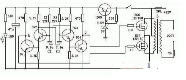
The following is a relatively easy to make inverter circuit diagram, can be 12V DC power supply voltage is reversed to 220V mains voltage, the circuit is driven by a multivibrator composed of BG2 and BG3, and then driven by BG1 and BG4 to control BG6 Work with BG7. The oscillating circuit is powered by the regulated power supply of the BG5 and DW groups, which can make the output frequency more stable. In production, the transformer can be used with a common dual 12V output mains transformer. According to the need, select the appropriate 12V battery capacity.
TL494 chip 400W inverter circuit diagram
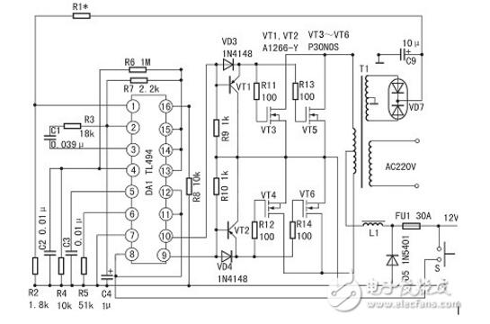
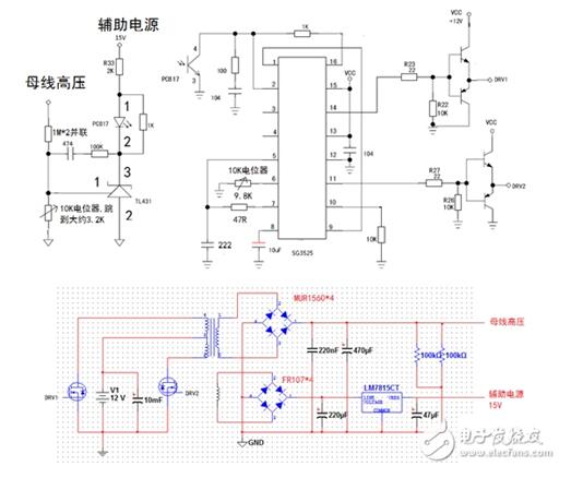
The transformer power is 400VA and the core uses 45&Times; 60mm2 silicon steel sheet. The primary windings are enameled wire with a diameter of 1.2mm and two wires are wound around 2&Times; 20 turns. Sub-sampling windings were made with 0.41mm enameled wire wound around 36 turns, center-tapped. The secondary winding is calculated as 230V, using a 0.8mm enameled wire wound around 400 turns. The switch tubes VT4 to VT6 can be replaced by any type of 60V/30A N-channel MOS FET tube. VD7 can use 1N400X series ordinary diodes. This circuit can work normally without debugging. When the positive voltage of C9 is 12V, R1 can be selected between 3.6~4.7kΩ, or adjusted with a 10kΩ potentiometer to make the output voltage rated. If the output power of the inverter is increased to approximately 600W, in order to avoid excessive primary current and increase resistive losses, it is advisable to switch the battery to 24V. A large-current MOS FET with a VDS of 100V may be used as the switch tube.
It should be noted that Ning can choose to use multiple pipes in parallel instead of using only one switch whose IDS is greater than 50A. The reason is that: one price is higher, and two drives are too difficult. It is recommended to use the 2SK564 with 100V/32A or three parallel 2SK906 applications. At the same time, the transformer core cross-section needs to reach 50cm2, the number of turns and the wire diameter are calculated according to the calculation method of the ordinary power transformer, or the transformer is replaced by the waste UPS-600. If you are powering a refrigerator or a fan, don't forget to add an LC low-pass filter. Using TL494 composed of 400W high power voltage regulator inverter circuit. It uses the TL494, VT1, VT2, VD3 and VD4 as the sink current drive circuit to drive two 60V/30A MOS FET switches. If you need to increase the output power, each circuit can be used in parallel with 3 to 4 switches, and the circuit will not change.
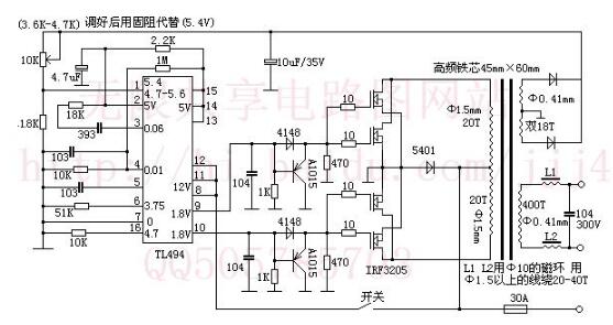
50HZ sine wave inverter circuit based on TL494
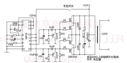
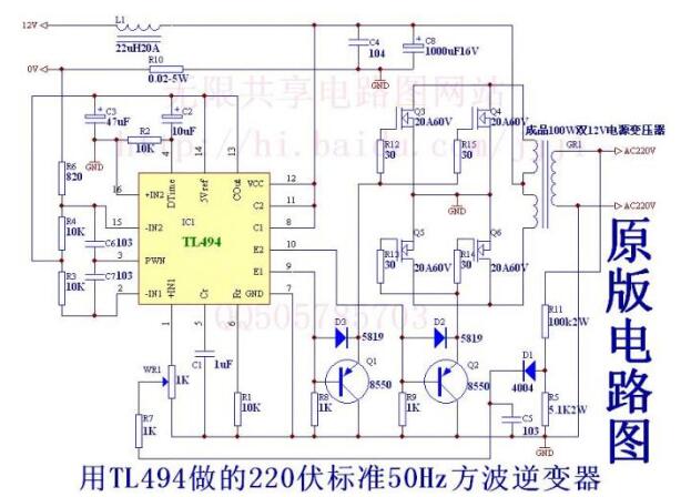
220 volt standard 50HZ square wave inverter based on TL494
555 as an inverter circuit: simple high-frequency inverter circuit
The 555 timer has low cost and reliable performance. It requires only a few external resistors and capacitors to implement multi-vibrator, monostable and Schmitt trigger pulse generation and conversion circuits. It is also commonly used as a timer widely used in instrumentation, household appliances, electronic measurement and automatic control. It includes two voltage comparators, three equivalent series resistors, one RS flip-flop, one discharge tube T and power output stage. It provides two reference voltages VCC/3 and 2VCC/3.
555 as inverter circuit two: home inverter circuit
The working principle of the circuit is shown in Figure 1. When the switch K1 is turned to the "inverter" position, BG1 is turned on, and an astable multivibrator composed of the time base circuit NE555 and peripheral elements starts to oscillate, and its charge and discharge time constants can be adjusted. If R1=R2 is selected, the duty ratio of the output pulse is 50%. The oscillation frequency of this multivibrator is f=1,443/(R1+R2+2W)C2. The component values ​​in the figure can adjust the oscillation frequency. At 50Hz, the oscillation pulse is output from the service leg. The waveform is a square wave. The square wave is coupled via C4, and the R3 and C5 integrals become triangular waves. This triangular wave passes R4 and C6 again. The second integration and the third integration of R5 and C7 , Become an approximate sine wave, coupled to BG2 through C8, amplified by BG2 and output on the L2 coil of B1. When the voltage at the upper end of L2 is positive, D4 ​​is cut off, D3 is turned on, BG4 and BG6 are turned off, BG3 and BG5 are turned on, and the current is from the positive electrode of the battery - L2-BG5 of the battery-the negative electrode of the battery; when the voltage at the upper end of L2 is negative, D3 Cut-off, D4 conduction, so that BG3, BG5 off, BG4, BG6 conduction, the current from the battery cathode -B2 L2-BG6 a negative battery. BG5 and BG6 alternately turn on and off. A positive and negative symmetrical sine wave is synthesized by the transformer B2 and sent to the inverter output sockets CZ1 and CZ2 by the L3 booster for use by the electrical appliance, and the LED1 (red) is turned on to indicate the inverter state. .
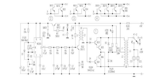
When the switch is turned to the “charged†position, the mains supply is stepped down by the transformer B2, full-wave rectified by D5, D6, and R11 current limit to charge the battery. At the same time, LED2 (green) is on, indicating the charging status.
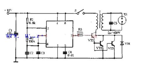
555 for inverter circuit three: typical inverter circuit
The figure is an inverter circuit composed of NE555, etc. It converts the 12V DC voltage of the battery to the 220V AC output voltage. In the circuit, NE555 is the oscillation circuit, the oscillation frequency is decided by the resistance value of R1, RP1 and C1, regulate the resistance of RP1, make it 50HZ. The NE555's 3-pin output pulse signal is applied directly to the base of VT2 and the other way is applied to the base of VT1 via the VT11 inverter. VT1 and VT2 are pulsed with a phase difference of 180°. The pulse voltage is transmitted through VT1 and VT2 carries on the shaping, then carries on the pulse amplification by VT3 and VT4, drives the power amplifier which is made up of VT5, VT7, VT8 and VT6, VT9, VT10. The power amplifier switching operation can convert the +12V battery voltage into a square wave voltage, which is converted into a 220V square wave AC output voltage via step-up transformer T1. VD1 and VD2 are surge absorption diodes, VT12, etc. are circuits that prevent the battery from over-discharging. The 78M06 provides the NE555 with a stable operating voltage of +6V.
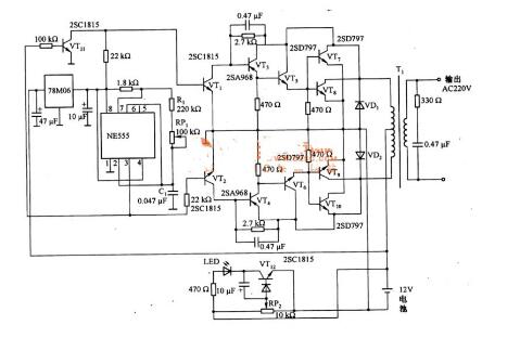
Pure sine wave inverter circuit 1
The following figure shows the circuit diagram of the previous stage. This circuit adopts the iris isolation feedback and works in the quasi-closed loop mode. When light load or no load, due to the transformer leakage inductance, the output may be over-voltage, easy to wear after the stage and capacitance. At this time, the duty cycle decreases and the output decreases. When the load increases, the circuit gradually enters the open-loop mode to ensure sufficient voltage and power output.
Pure sine wave inverter circuit two
The following figure shows the circuit diagram
The advantages of this circuit:
1. The circuit is very simple and may be the world's simplest discrete SPWM circuit
2. Single-supply wide voltage supply (10V-30V)
3. The maximum output duty cycle is high. The maximum duty cycle during simulation is close to 100%. This will result in a high utilization of the bus voltage. The bus voltage of 340V is sufficient to generate 230V sinusoidal AC power.
4. Isolated output, less interference by peripheral circuits.
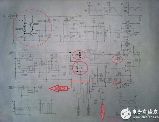
As shown, the LM7809 reduces the battery voltage to a stable 9V, which allows the circuit to operate in a wide power supply (10V-30V). The 2N5551 and 2N5401 components in the red circle in the upper left corner form a virtual dual power supply, changing the positive 9V. Positive and negative 4.5V dual power supply.
The NE555 and its surrounding components form a high-linearity triangular wave oscillator with a frequency of approximately 20 KHz. As shown in the figure, the triangle waves of 3 V and 6 V can be obtained at the NE555 feet 2 and 6.
IC1 is composed of LM324, IC1A and peripheral components 50Hz power frequency sine oscillator, generates a sine wave amplitude 4.5V (for the virtual ground), a potentiometer potentiometer this sine wave amplitude is divided to 3.5V. IC1B and IC1C and Peripheral components form a precision rectifying circuit that converts the sine wave into a 3V amplitude bow wave. The first wave is compared with the triangle wave of NE555. Although the amplitudes of the triangle wave and the first wave are all the same, they are 3V, but the lowest potential of this skull wave is 1.5V higher than that of the triangle wave. Therefore, the IC1D and peripheral components compose a subtraction circuit. The whole head wave is down-regulated by 1.5V, so that the triangular wave and the first wave can be compared. The LM393B performs a comparison operation to generate a SPWM wave of the same phase. This wave is sent to the synchronizing square wave output of the sinusoidal-square wave converter composed of the LM393A. Code circuits such as the CD4081 are encoded to generate the final drive power SPWM signal. Two 20K resistors and 47P capacitors are used to generate a dead zone in the high frequency arm. SPWM1 and SPWM2 are used to drive the high frequency arm, and 50HZ1 and 50HZ2 are used to drive the power frequency arm.
One of the ingenious places in this circuit design is the conversion of virtual ground and field. Before the LM393A, the circuit was working in virtual ground, and the circuit after the LM393 turned into the field. Because 4.5V AC (for virtual ground) is a 9V pulse for the field. The LM393B peripheral circuit is similar.
Pure sine wave inverter circuit three
The following figure shows the H-bridge circuit diagram of a full hardware pure sine wave inverter.
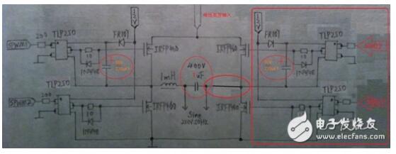
The IRFP460 in the lower arm is driven directly by the diaphragm, and the IRFP460 in the upper arm is driven by the bootstrap capacitor + diaphragm. The working principle is briefly described: When the lower arm is on, the midpoint of the power tube of the high-frequency bridge is equivalent to ground. At this time, the 220uF bootstrap capacitor is charged by the FR107 and the lower arm tube. When the lower arm turns off, the upper arm is turned on, 220uF. The capacitor is isolated from ground. When the TLP250 internal triode is turned on, it is equivalent to applying a voltage between the GS of the upper arm tube, so the upper arm tube can be turned on and off under the control of the corresponding TLP250.
A 1mH inductor and a 400V 1uF capacitor are used to complete the task of high frequency filtering, turning the high frequency SPWM square wave into a 50Hz sine wave.
Pure sine wave inverter circuit 4
Pure sine wave inverter power supply circuit made with single-chip microcomputer
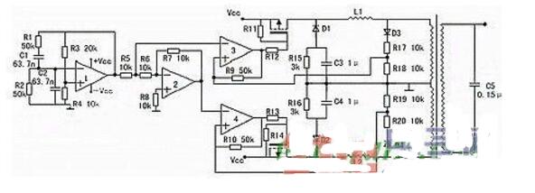
The above is a high-efficiency sine wave inverter electrical diagram, which is powered by a 12V battery. First use a voltage doubler module to provide power to the op amp. ICL7660 or MAX1044 can be selected. Op amp 1 produces a 50Hz sine wave as the reference signal. Op amp 2 acts as an inverter. Op amp 3 and Op amp 4 are used as hysteresis comparators. In fact, the operational amplifier 3 and the switch 1 constitute a proportional switching power supply. The same applies to the amplifier 4 and the switch 2 . Its switching frequency is not stable. When the output signal of the operational amplifier 1 is positive phase, the operational amplifier 3 and the switch tube work. At this time, the output of op amp 2 is negative. At this time, the potential of the positive input terminal of the operational amplifier 4 (constant zero) is always higher than the potential of the negative input terminal, so the output of the operational amplifier 4 is always 1 and the switch tube is closed. When op amp 1 output is negative, the opposite is true. This realizes that the two switch tubes work alternately.
When the reference signal is smaller than the detection signal, that is, the signal of the negative input terminal of the op amp 3 or 4 is higher than the signal of the positive input terminal by a small value, the comparator outputs 0, the switch is opened, and the detection signal is rapidly increased accordingly. When the detection signal is increased, When the reference signal is a little higher than the reference signal, the comparator outputs 1 and the switch is off. It should be noted here that the comparator has a positive feedback process when the circuit is turned over, which is a feature of the hysteresis comparator. For example, if the reference signal is lower than the detection signal, the reference signal is immediately higher than the detection signal by a certain value at the same instant as their difference is constantly approaching. This "a certain value" affects the switching frequency. The bigger it is, the lower the frequency. Here it is selected as 0.1~0.2V.
The purpose of C3 and C4 is to allow the freewheeling current of the higher frequency switch to pass through, and to generate a larger impedance to the lower frequency 50Hz signal. C5 is calculated by the formula: 50=. L is generally 70H, it is best to test when making. So C is about 0.15μ. The ratio between R4 and R3 must be strictly equal to 0.5. Large waveform distortion is obvious. Smaller ones cannot start vibration, but they are rather large and must not be small. The maximum current of the switch is: I==25A.
GPON (Gigabit-Capable Passive Optical Networks) technology is the latest generation of broadband passive optical integrated access standards based on the ITU-TG.984.x standard. It has many advantages such as high bandwidth, high efficiency, large coverage, and rich user interfaces. It is regarded by most operators as an ideal technology to realize broadband and comprehensive transformation of access network services. GPON was first proposed by the FSAN organization in September 2002. On this basis, ITU-T completed the formulation of ITU-T G.984.1 and G.984.2 in March 2003, and completed G.984.1 and G.984.2 in February and June 2004. 984.3 standardization. Thus finally formed the standard family of GPON.
GPON is a gigabit passive optical network or Gigabit passive optical network. GPON technology is the latest generation of broadband passive optical integrated access standards based on the ITU-TG. 984.x standard. It has high bandwidth, high efficiency, and large Many advantages such as coverage and rich user interface are regarded by most operators as an ideal technology to realize broadband and comprehensive transformation of access network services.
GPON technology allows operators to provide specific services that their customers need to provide in a targeted manner based on their market potential and specific regulatory environment. GPON technology and equipment are relatively complicated. GPON bears the advantages of multi-service with QoS guarantee and strong OAM capabilities to a large extent at the cost of technology and equipment complexity, which makes the cost of related equipment higher. With the development and large-scale application of GPON technology, the cost of GPON equipment will drop accordingly.
Gpon 1Ge Ont,Gpon 4Ge Ont,Gpon Ont,Gpon Onu,WLAN Port,Vlan
Shenzhen GL-COM Technology CO.,LTD. , https://www.szglcom.com