This paper aims at the random and fixed clock jitter of high-speed fully-differential op amps and high-bandwidth 14-bit analog/digital converters in a full-range signal path system, and specifically analyzes and studies ultra-low noise and clock jitter filtering techniques. Research selected dual-cascaded PLNaTInum architecture, configuration of high-performance voltage-controlled oscillator (VCXO), a good realization of the role of noise reduction and clock jitter filtering.
0 PrefaceWith the development of electronic information technology, data transmission has played an important role in military aviation, wireless network infrastructure construction, testing and measurement. The clock is an indispensable and critical part of communication terminals, transmission and reception quantification and synchronization standards. During signal transmission, the crystal reference clock itself has low jitter, but the random jitter and periodic jitter (PJ) due to IC, switching power supply noise, data or clock line disturbances have relatively large clock quality and system performance. influences.
A typical signal path design is composed of signal sensors, analog signal processing blocks, data converters, interfaces, and digital processing blocks. To make the system perform fully, the main components used in the path must meet the relevant requirements. Taking an analog/digital converter as an example, a system designer wants a signal-to-noise ratio (SNR) of not less than 60 dB, so a 14-bit data converter with a high frequency bandwidth and a frequency requirement of up to 1 Gpsp can be used. In the process of system design and use, positioning sampling using data signals and reference clocks is an important part, and high-precision clock generation technology has become one of the technologies to be developed. Under normal circumstances, the design uses a single phase-locked loop (PLL) clock generator in the work process, the multiplier will amplify the clock jitter, while introducing its own jitter, can not meet the average jitter index Jrms "1ps @ (12KHz ~ 20MHz ) Requirements.
In order to realize the ultra-low noise precise clock, the author has studied and discussed the cascading PLL clock jitter filtering technology, and did some analysis on the system clock jitter.
1. Dual-cascade PLL noise reduction filter designWhen the input noise is large, the system has a narrow loop bandwidth, such as tens of Hz to several hundred Hz. With the aid of a local high-performance voltage-controlled oscillator, such as VCXO, OCXO, etc., the noise of the reference clock can be input. The filter is clean and the PLL outputs a clock signal that is superior to the jitter performance of the reference clock.
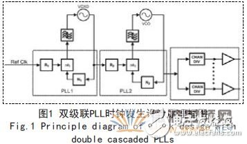
As shown in Figure 1, the clock is generated using a cascaded double PLL architecture to clear the signal jitter. In the figure, after the VCO output, a clock distribution circuit is continued.
The first PLL uses a very narrow loop bandwidth to lock the frequency of the external VCXO to the input reference clock signal. The extremely narrow loop bandwidth can suppress most of the phase noise in the reference clock signal, making the phase noise of the VCXO the dominant noise component. The frequency-locked VCXO is input as a reference clock to the second PLL, which uses a larger loop bandwidth to lock the built-in VCO. This large loop bandwidth means that both the phase and frequency of the VCO are locked to the VCXO, so the noise of the VCXO becomes the main component.
For signal phase noise above the loop bandwidth, the phase noise of the internal VCO and the output divider and driver will determine the phase noise of the output signal.
Equation (1) shows that the total noise is the weighted sum of the reference clock noise, PLL noise, and VCO noise:
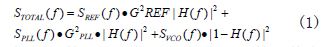
The weighting function H(f) is a low-pass closed-loop transfer function that includes parameters such as charge pump gain, loop filter response, VCO gain, and feedback path (N) counter. This equation shows the noise model at the output of each stage PLL shown in Figure 1. The gain of the reference clock signal noise (GREF) and the gain of the PLL noise (GPLL) are also a function of the specific loop parameters. Here we do not derive these expressions of gain and closed-loop response H(f) as conclusions. In general, the parameters of the composite device that make up H(f) and the gain values ​​given in the equations can all be adjusted by the designer. The standard chosen is the total noise at the output of the synthesizer (STOTAL(f). ))minimize. In this case, minimizing means minimizing the total noise after synthesis. When this noise equation is used for PLL2, SREF(f) represents VCXO noise. SPLL(f) and SVCO(f) are determined by the characteristics of the device, but SREF(f) depends on the VCXO chosen by the designer.
2. Technical Analysis and Simulation2.1 Phase noise analysis
The author's experiment and simulation parameters are as follows, PLL1:
125MHz ordinary crystal reference input, R=120, N=120, 100uA charge mercury current; PLL2: NBXHGA019 125MHz reference crystal input, R=2, N=10, internal VCO divider set to 2, loop bandwidth to 366kHz, 4th-order loop filter with phase margin of 85.5 degrees, charge mercury current of 3.2mA, output mode of LVPECL, and synchronous output frequency division selection are different, and a random selection is made between 2 and 510.
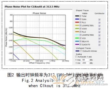
Figure 2 shows the phase noise analysis with an output clock frequency of 312.5 MHz. The phase noise is determined by the VCXO noise of the reference input, the PLL open and closed loop noise, and the internal VCO noise. The figure shows that the total phase noise has a phase shift of -113.09 dB/Hz at 1.000 kHz, -128.46 dB/Hz at 100.000 kHz, and -155.22 dB/Hz at 10,000.000 kHz.
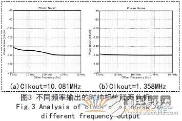
Figure 3 shows the phase noise analysis of the clock when the output clock frequency is 10.081MHz and 1.358MHz. Compared with the three, the phase noise gradually decreases with the increase of the output frequency, making the signal noise in the transmission process. Than to reduce the system to less than 60dB, to meet the design needs.
2.2 RMS jitter characteristics
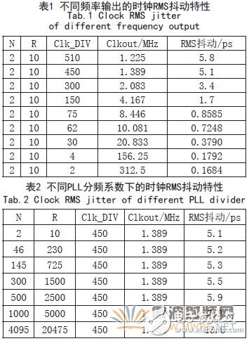
Mean (RMS) jitter is an important parameter that characterizes clock jitter. As shown in Table 1, the RMS jitter of different frequency outputs obtained by the author in the jitter detection of the sampling points of 1001, the lowest 1 kHz and the highest 10 MHz. With the same PLL frequency division factor, the measured RMS jitter gradually decreases as the frequency increases. When the frequency is 312.5 MHz, the jitter is 168.4 fs, compared with 0.5 pf that provides the reference clock. With great improvements and improvements. Table 2 shows the RMS jitter of the output clock under different frequency division ratios. It can be clearly seen that the jitter increases exponentially with the increase of the coefficient.
From simulation and research, we can see that the dual-cascaded PLL architecture clocks are designed to achieve multiple-frequency synthesis and very low phase noise while achieving jitter filtering below 300 fs (RMS jitter as low as 1.8ps@10KHz~5MHz). . The ultra-low jitter, low-power clock generation technology satisfies analog-to-digital conversion sampling and clock and signal guarantee conditions for signal path design. At the same time, this type of design can also be applied to wireless base stations, microwave communications, and 100GE data communications.
In-ear earphones are sometimes referred to as earbuds, and they refer to earphoees that are small enough to fit into the ear. The Sport Earphone are written with L and R, L is left for the left channel, and R is the right for the right channel. In principle, the thinner the earmuffs, the more comfortable they are. However, the thin earmuffs will be less soundproof.
Correct use:
1: Set the volume of the source to the minimum.
2: Insert the 3.5mm plug of the in-ear earphone into the earphone jack.
3: Adjust the volume to a position that sounds comfortable. In-ear earphones are not recommended for driving motorcycles, bicycles, operating machines, and jogging, as you may affect your judgment of potential hazards.
4: Do not open the volume too much during use.
5: When pulling the earphone plug, you should pinch the hard plastic part of the back end of the plug and pull it out, instead of pulling it straight out through the wire.
6: Avoid excessive bending of the wire for a long time.

In Ear Headphones,Sport Earphone,In Ear Earphones,Zipper In Ear Headphones
Shenzhen Linx Technology Co., Ltd. , https://www.linxheadphone.com