Abstract: MIMO technology, multi-carrier technology and link adaptation technology are the most worthy physical layer technologies for future mobile communication systems. MIMO technology has excellent performance in improving system spectrum utilization, and multi-carrier CDMA technology can effectively combat frequency selective fading. Combining MIMO technology with MC-CDMA scheme to form a space-domain multiplexing MC-CDMA system will be very important To a certain extent, the performance and capacity of the system are improved, the information transmission rate is more effectively improved, and the task of designing and implementing the baseband signal processing platform of the FPGA-based spatial domain multiplexing MIMO MC-CDMA system is completed [1]. In this paper, a hardware simulation model is used to simulate the MIMO channel, which realizes the joint debugging and functional verification of the system. Compared with the software simulation results, the performance is good.
1 MC-COMA modulation and demodulation hardware implementation
1.1 Scheme design
According to the basic principles of MC-CDMA modulation and demodulation, the modulation process is divided into three functional modules: symbol replication, frequency domain spreading, and carrier modulation in the design of the scheme, and the demodulation process is divided into carrier demodulation, despreading, and frequency. The domain merges three functional modules. Taking into account the neatness of the code and the requirements of the operation speed, the pipeline operation mode is adopted in the design.
According to requirements, the number of subcarriers in the design scheme in this paper is 32, and the spreading code is generated by an OVSF code generator with a length of 32. By setting the parameters of the OVSF code generator, one of 32 different codewords can be selected for spreading To distinguish the data of different users. The timing relationship between each module is realized by control signals such as ens, and the back-end module is triggered only after the operation of the front-end module is completed, thereby achieving pipeline operation. For more information, please log in to the electronic enthusiast website (http: //)
MC-CDMA modulates the relationship and signal flow between all program modules. The MC-CDMA module is the top module, the three functions in the second row are first-level submodules, and the functions in the third row are second-level modules. The data symbols entering the MC-CDMA modulator are first copied N times. In this system, N = 32. The Copy32 subroutine module is used to realize the symbol copy function in multi-carrier modulation. The copied data is sent to the frequency-domain spreading module sPreading, spread through the OVsF code sequence with a length of 32, and then sent to the IFFT32 arithmetic module to realize the conversion from frequency domain to time domain to complete MC-CDMA modulation.
1.2 Realization of spreading in frequency domain
In spread spectrum communication systems, the principle is to use the spread spectrum sequence to expand the user's original signal. At the receiving end, in order to restore the original signal, the same synchronous spreading sequence as the transmitting end is used to correlate with the received signal. MC-CDMA utilizes the cross-correlation of spreading sequences for multi-user communication. Spreading sequences play an important role in MC-CDMA systems.
1.3 FPGA implementation of FFT / IFFT
The FFT / IFFT design in this article refers to the data sheet [2] of Altera ’s FFTIP core. Through actual testing of the IP core, it can be seen that the valid data is delayed by 4 clock cycles of the START signal. In this system, the control signal and valid data from the front-end module are input to the FFT / IFFT transform module synchronously, so 4 cycles need to be registered for the input data. The input data buffer module is used to register the input data. The timing control unit is used to ensure the timing alignment in the module. FFT / IFFT arithmetic unit is based on Altera Megacore IP core. The main parameter settings of FFT / IFFT IP core are shown in Table 1. The conversion length is 32, and the parallel pipeline FO structure is adopted. In order to save the consumption of slices resources, the block RAM resources on-chip are selected to the maximum extent. Table 1 shows the resource consumption of the integrated FFT & IFFT module. From the comprehensive report, the maximum execution speed can reach 268 MHz.
2 System overview
2.1 System verification scheme
Based on the design methods of the transmitter and receiver of the 2-transmit and 3-receive MIMOMC-CDMA baseband system proposed above, after the RTL code writing and functional verification of the transmitter and receiver are implemented respectively, the transmitter and receiver are combined Tests were conducted to verify the basic functions of the 2-transmit and 3-receive MIMOMC-CDMA baseband system designed and implemented in this paper.
The channel processing of the 2-transmit and 3-receive MIMO system is similar to the hardware emulation MIMO channel module. The signals xl, x2 from the two transmitters of the transmitter interact with the channel matrix and add Gaussian white noise to obtain 3 data: r1, r2, r3 , Sent to the 3 receiving antenna ends of the receiver. The receiver detection algorithm is based on the assumption that the 6 parameters h11 to h33 of the 2 transmit 3 receive MIMO channel matrix have been correctly estimated. The channel parameters in the joint debugging of the system come from the MATLAB simulation system of 32 sub-carriers, two-transmission and three-reception MIMOMC-CDMA. First, the parameters of the simulated channel on each carrier are obtained. At this time, the channel parameters are complex floating-point data; In the environment, write a program that converts any complex number into hexadecimal data with a setpoint structure and bit width, converts these complex channel parameters into hexadecimal numbers that Verilog encoding can recognize, and these channels are implemented in this paper. The parameter is converted into a hexadecimal number with a bit width of 16, where the real part and the imaginary part are represented by high 8 bits and low 8 bits, respectively. Among these 8 bits, 1 bit is a sign bit, and the other 7 bits are preset channel parameter values, of which 2 bits are integer bits and 5 bits are decimal bits.
2.2 Design and implementation of system clock management unit
In order to meet the requirements of synchronous timing design, global clock resources are generally used in FPGA design to control the designed main clock to achieve the lowest clock jitter and delay. The implementation of the clock management unit in this article also follows this principle. The system clock generation structure module designed in this paper uses 3 Altera OCMIP cores to generate 6 kinds of frequency division of the product vibration clock. The input clock is used to drive the second and the first after passing through an IBIJFG in the first DCMIP core module Three OCMIP core modules.
2.3 System verification results
The simulation conditions are set as follows: unit bit signal-to-noise ratio EbNo = 4, system bandwidth B = 20 MHz, OVSF spreading code word number K = 31, channel parameter group simulation channel when ch = 2, length of long source random signal It is L = T × len = 2 000 × 15 = 30 000, single user, AWGN channel. ErrorN is the number of error codes collected by the receiver. Figure 1 is the simulation result of the system joint debugging when using QPsK modulation. The number of errored bits obtained by the sink module ErrorN is 602, BER == 602/30 000 = 0.020 067, and the simulation result when it is close to EbNo = 4 is 0.020 05 .
As the modulation order increases, the performance of the system will decrease, and the higher order modulation will require higher system hardware. Figure 2 shows the chip resources occupied by the system using the synthesis tool of the Altera Quartus II 6.0 simulation platform. The chip used in the simulation is the same as the chip on the DE2 development board, all of which are Altera Cyclone II from Altera Corporation. Because the multiplication and complex multiplication operations involved in the operation process are simplified, and the fixed value module on the chip is used as efficiently as possible, which greatly reduces the resource consumption.
This paper first proposes a system joint debugging scheme framework for a 2-transmit and 3-receive MIMO MC-CDMA baseband system, uses hardware emulation MIMO channel modules to realize the connection between the transmitter and the receiver, and designs a system clock management unit that spans 6 clock domains. The clock synchronization between each module is realized, and the design implementation method and function simulation results of the clock management unit are introduced in detail. The FPGA baseband system was jointly debugged and compared with the MATLAB simulation results. The functions of the transmitter and receiver were verified. The RTL code of the entire baseband system was successfully downloaded to the chip of the DE2 development board. For more information, please log in to the electronic enthusiast website (http: //)
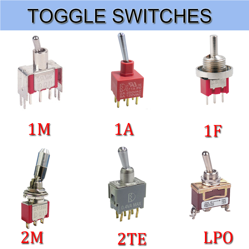
Toggle switches, also called On Off Toggle Switches, is often used as the switching device of the equipment stalls. Meanwhile, we are also offer our customers Key Switches , Metal Switches, Automotive Switches, Push Button Switches, etc.
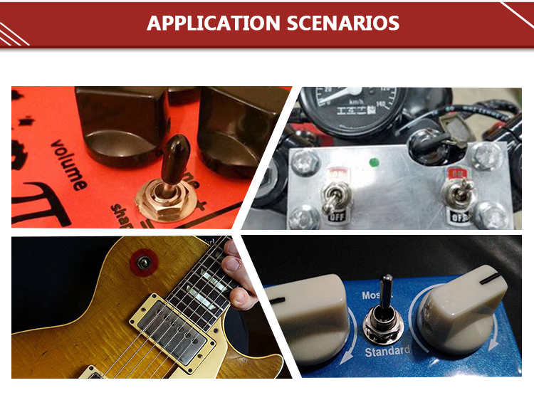
The Electrical Toggle Switches is a manually controlled Toggle Switches similar to the dial switch. Most of this Latching Toggle Switches are widely used in on-off control of AC and DC power circuits, and are less commonly used in circuits of several kilohertz or up to 1 megahertz. Let's take a look at the following.

1. Splash-proof knob button switch
The panel is installed with a splash-proof `O` ring seal, and the knob is a ball. It is a splash-proof ball button knob switch. Its terminals are in a straight line and the bottom of the terminals is sealed with epoxy resin. Strong corrosion resistance, suitable for automotive parts
2. Vertical Mount Right Angle Toggle Switch
The vertical mounting of the terminals and the terminal pins are right-angled, so it is a vertically mounted right-angled toggle switch. Its contacts are gold-plated and highly reliable. Mostly used in anti-theft devices, alert system.
3. Bipolar single toggle switch
At the same time, the switch breaks the phase line and the N line and controls one branch. Therefore, it is a bipolar single toggle switches. The contacts are in 3PDT form and are used for multimedia speakers and stereos.
4. Standard surface mount unthreaded toggle switches
The terminal adopts the standard mounting mode. Its sleeve has no thread. It is called a standard surface mount screw-less switch. The contacts are SPDT and its electrical life is as high as 55,000. Used for medical equipment
5. Horizontally mounted right-angle toggle switch
Compared to the vertical switch, it only changes direction to horizontal, so it is horizontally mounted right-angle toggle switch. The contacts are double-pole double-throw and the bottom of the terminal is Epoxy Seal. Mostly used for computer peripherals.

Toggle Switches
Toggle Switches,Toggle Switch On Off,Toggle Switch Autozone,Toggle Switch Home Depot
YESWITCH ELECTRONICS CO., LTD. , https://www.yeswitches.com