This paper introduces the PMSM drive control system based on ZynqSoC. The control system uses a combination of ARM and FPGA to achieve high performance and high integration control algorithm. In the FPGA part of the system, the PMSM current loop vector control algorithm with high computational parallelism and high computational performance is realized. The ARM part realizes the speed control algorithm and position control algorithm with strong portability and many kinds of algorithms. The experimental results show that the system has high performance and scalability, and can be easily applied to different practical projects.
In industrial control systems such as robots, robotic arms and CNC machine tools, the drive control of permanent magnet synchronous motors (PMSM) has always been the core of such control systems. With the development of industrial technology and the increasing use of PMSM, the demand for performance and accuracy of PMSM drive control systems is increasing. In order to meet the requirements of high performance, high precision, etc., some scholars use high-performance DSP as a hardware and software solution, and some scholars use ARM microcontrollers as system solutions, such as the control system implemented by STM32 [3]. Due to the increasing complexity of the PMSM control algorithm and the increasing requirements of the controller for the performance of the controller, foreign scholars have proposed the use of FPGA as the drive control system solution for PMSM [4], and the effect is remarkable.
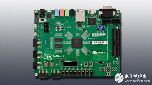
The control core board used in this article is the ZedBoard development board equipped with the Zynq7000 series chip XC7Z020CLG484. Using such products, you can use ARM to perform fast operating system migration [7] and human-computer interaction software development under the premise of giving full play to the advantages of FPGA parallel computing. The development scheme of this paper is to implement different control algorithm modules on ARM and FPGA respectively. This scheme improves the control performance and portability of the system while combining the advantages of ARM and FPGA. Click to see more exciting content.
1 Introduction to the control systemThe common PMSM drive control system can be divided into three levels of control modules: current loop, speed loop and position loop, as well as electromechanical sensor signal processing interface, data monitoring, human-computer interaction and so on. The current loop control scheme mostly uses a vector control algorithm. By detecting the phase current value of PMSM, the stator is decomposed into excitation current and torque current by coordinate transformation to achieve respective closed-loop control [8]. The speed loop and position loop controller are commonly used as PID controllers.
The structure of the control system is shown in Figure 1. According to the type of function, the system components can be divided into several parts of the electromechanical interface component, the vector control algorithm component and the control layer component.
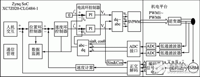
Figure 1 Control system structure
1.1 Electromechanical interface components
The electromechanical interface component is mainly to realize the functions of signal receiving, transmitting and signal processing of modules such as machinery and circuits. The component's signal input capture module provides data in a specified format for subsequent algorithm layers, and the signal output module provides standard controllable signal waveforms for the electromechanical execution circuitry. Specifically, the component consists of the following modules:
1 Encoder quadrature decoding module. The module implements processing of the encoder signal, and captures the output waveform of the encoder to calculate data such as motor speed and rotor position.
2 ADC interface module. This module implements the transmission protocol of the A/D converter. This system uses an A/D converter with an SPI interface, so the module implements the SPI communication protocol.
3 PWM generator. The module performs pulse width tunable waveform (PWM) generation, which produces six PWM signals for driving the inverters designed herein.
1.2 Vector Control Algorithm Components
The vector control algorithm component performs the current loop correlation algorithm of PMSM. This component includes the following modules:
1 Sin&Cos module. The module performs the calculation of the electrical angle value of the rotor to the sine and cosine values.
2 Space coordinate conversion module. The module equivalents the control target PMSM of the system into a control algorithm and a simpler DC motor. It mainly includes three-phase two-phase coordinate transformation and synchronous rotary transformation modules to realize the stator three-phase current decoupling into torque current. The calculation process of iq and excitation current id.
3 SVPWM module. This module implements functions such as generation of space vector PWM signals.
1.3 Control layer components
The control layer component implements the three-loop control of the PMSM, and mainly includes the following modules:
1 controller module of current loop torque current iq and excitation current id;
2 speed loop, position loop controller, and rotor speed, position calculation and other modules;
3 Auxiliary control and test related modules, mainly to achieve human-computer interaction, debugging data acquisition and other functions.
2 system hardware platform designThe hardware platform of the embedded drive control system is composed of four printed circuit boards (PCBs), and its composition is shown in FIG. 2. The PCB board consists of a ZedBoard development board, an FMC interface board, a signal processing board, and a driver board.
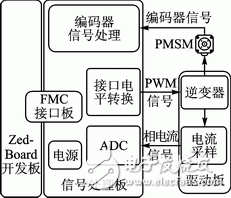
Figure 2 system board composition
3 system software designAccording to the block diagram of the drive control system, the software algorithm module of the system can be divided into ARM or FPGA according to the algorithm parallelism, performance requirements and portability requirements. The control system uses FPGA to implement vector control current loop to improve algorithm parallelism and calculation frequency. ARM is used to implement algorithms such as speed loop, position loop and human-computer interaction to ensure the convenience of software development and the portability of the algorithm. The ARM and FPGA communication in the system is implemented using Zynq on-chip high-performance bus (AXI HP) and interrupt signals. System software block diagram slightly - editor's note.
3.1 ARM and FPGA communication design
The inter-core communication problem between ARM and FPGA is the top priority of Zynq application development. The inter-core communication bus AXI HP can use the form of direct memory access (DMA) for data transmission. The maximum bit width of the bus is 64 bits, and the theoretical communication bandwidth. Up to 1 200 MB/s. The communication scheme used is the way that the interrupt signal and the AXI HP bus work together. The interrupt signal realizes the synergy between ARM and FPGA control cycles. The AXI HP bus provides high bandwidth communication speed for ARM and FPGA. The system uses the AXI HP bus to directly read and write ARM data space in the form of DMA, so ARM does not need to manage communication timing during the control algorithm cycle.
The inter-core communication timing diagram of the system is shown in Figure 3.
The data transmission in the figure occurs after the FPGA and ARM algorithm software completes the data processing. The data processing here includes the following two aspects:
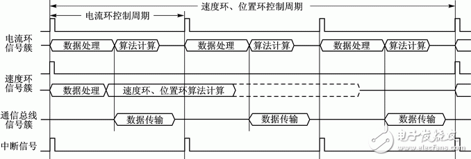
Figure 3 ARM and FPGA communication timing diagram
1 FPGA-side data processing includes the acquisition and processing of sensor signals such as encoders and A/D converters, as well as the collection and processing of important variable data during the operation of the current cycle control algorithm in the previous cycle.
2 ARM-side data processing includes the saving of the current given command of the speed loop output, the current loop feedback data processing of the previous cycle, and the analysis of human-computer interaction command data.
The data transmission of the communication signal cluster described in FIG. 3 is mainly to complete the operation of writing the FPGA data into the memory space accessible by the ARM and the data of the FPGA reading the specified memory space of the ARM. The interrupt signal involved in Figure 3 is initiated by the algorithm module on the FPGA. The main function is to synchronize the running timing of the FPGA and ARM. Through the data transmission and interrupt signals of the above AXI HP bus, the data interaction function between ARM and FPGA can be realized. The bus frequency is 90 MHz, and the data transmission bandwidth is 284 MB/s.
3.2 FPGA part code design
The system uses an FPGA (Xilinx's ArTIx7 series) embedded on the controller XC7Z020 chip, with a total resource of approximately 1.3 M logic gates. In this system, the current loop control frequency is 16 kHz, and the algorithm block diagram of its implementation is shown in Figure 4.
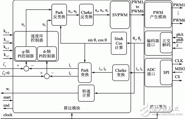
Figure 4 FPGA implementation software system block diagram
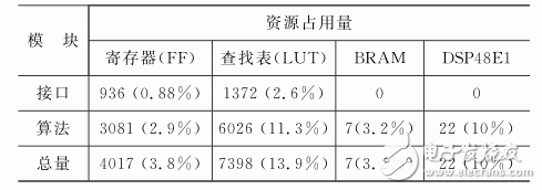
The software implemented on the FPGA includes two parts: algorithm and interface. The data part of the algorithm part is 16-bit Q15 fixed-point number. This part of the code completes the function simulation and verification of the code through the Xilinx tool ISE14.7. Each module occupies the total resources of the FPGA. The amounts are listed in Table 1. The algorithm code runs at a clock frequency of 90 MHz, and the algorithm calculation takes 5.7 μs. It can be seen that the computation time is sufficient to meet the 16 kHz current loop control frequency used by the system.
Table 1 FPGA algorithm resource occupancy
3.3 ARM part code design
The software program running on the dual-core ARM CortexA9 of this system mainly includes two parts: control component and auxiliary component. The control component runs in the interrupt service program to meet the timing requirements of the algorithm for the control cycle; the auxiliary component runs in the background cycle program to implement functions such as human-computer interaction interface management and system monitoring.
The interrupt service program of the system software is shown in Figure 5. The interrupt signal of the interrupt service program is sent by the vector control algorithm module of the FPGA.
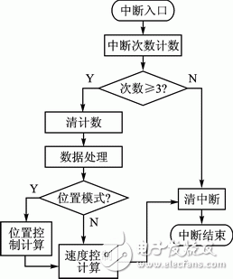
Figure 5 Software flow running on ARM
The data processing flow in the figure includes the following parts:
1 Human-computer interaction data processing. Realize user command parsing, system running command given and other functions. The main operating modes of the system include speed mode and position mode. The running commands include the given motor rotation position, rotation speed and so on.
2 Current loop feedback data analysis and processing. This link realizes the monitoring of the algorithm running on the FPGA, and encapsulates the motor operation data, so that the human-computer interaction component performs data transmission and the like.
3 Current loop command saves the given data. This link is mainly to process the output data of the speed controller of the previous cycle to ensure that the data can be accurately transmitted to the FPGA.
After the data processing is completed, the software runs to the core controller. The position loop controller used in this step is a proportional controller, and the speed loop controller is an integrated anti-saturation PI controller. After parameter tuning, the software algorithm can meet the requirements of system control accuracy and so on.
4 Experimental analysisThe system uses the Xilinx development tool suite ISE14.7, Vivado 2014.2 and SDK to implement code development and project management. Among them, ISE 14.7 is used to complete FPGA code development, algorithm function simulation verification, etc. Vivado 2014.2 is used for project management and Zynq ARM side startup file configuration, etc. SDK is used for ARM end application development work.
The experimental platform of this system contains the following parts:
1 PMSM motor with 2500 line encoder, motor parameters are listed in Table 2.
2 Motor drive board, signal processing board, FMC interface board, linear power supply for supplying DC bus voltage of the drive board.
3 ZedBoard development board equipped with XC7Z020CLG484 chip.
Figure 3-1 shows the speed and current response of the motor given the speed step value of the 400 SM/min of the PMSM drive control system. The speed response of the system is not over-adjusted, no static difference, and the current response is rapid. It can be seen that the PMSM control system has good control performance and control precision.
Table 2 Experimental platform PMSM parameters

Conclusion
This paper introduces a Zynq-based PMSM drive control system and introduces the design of the on-chip bus communication scheme for heterogeneous multi-core control systems. The system fully combines the advantages of ARM and FPGA in the application development of embedded systems, realizes human-computer interaction and portability algorithms on ARM, and realizes algorithms with high parallelism and high performance requirements on FPGA.
The feasibility and convenience of using PMnq to realize PMSM control system are verified by experiments. It shows that this scheme can not only improve system control performance, improve control precision and bandwidth, but also realize complex algorithm verification based on high performance controller. Humanized human-computer interaction and other functions, the system's control performance and scalability have been greatly enhanced.
Editor's Note: This article is an abbreviated version of the journal. The full text can be found on the website of this journal.
references
[1] Chen Yinghao. Application of PMSM vector control based on DSP in elevator control [J]. Microprocessor, 2010 (3): 105107.
[2] Li Changhong. Research on the maximum torque current ratio control method in PMSM speed control system [J]. Journal of China Electrical Engineering, 2005, 25(21): 169174.
[3] Zhang Wei. ARM-based PMSM control system design [J]. Microcomputer Information: Embedded and SOC, 2010, 26 (112): 7071.
[4] Mohamed Wissem Naouar. FPGABased PredicTIve Current Controller for Synchronous Machine Speed ​​Drive [J]. IEEE TRANSACTIONS ON POWER ELECTRONICS, 2008, 23 (4): 21152126.
[5] Li Huxiu. High-precision speed detection of permanent magnet synchronous motor based on FPGA + ARM [J]. Combination Machine Tool and Automatic Machining Technology, 2012(11): 5356.
[6] Xilinx. Zynq7000 All Programmable SoC Technical Reference Manual [EB/OL]. [201411]. Http://TIon/user_guides/ug585Zynq7000TRM.pdf.
[7] Fang Huaqi. Multi-verification operating system TOPPERS/FMP transplantation research [J]. Single Chip Microcomputer and Embedded System Applications, 2013(12): 47.
[8] Chen Boshi. Electric drag automatic control system - motion control system [M]. 3 edition. Beijing: Mechanical Industry Press, 2003: 190214.
FTTH Fiber Optic Splice Tray is designed to provide a place to store the fiber cables and splices and prevent them from becoming damaged or being misplaced. It is also called a splice enclosure or splice organizer. This device does not contain any technical functions, and the design is simple. Also, Fiber Optic Tray has a very low price for people to afford. However, the importance of fiber splice tray for protecting fibers is significant. And the skills needed for using a fiber splice tray is not as simple as you think.
Made by industrial high-quality ABS plastic, Fiber Optic Cable Tray is provided to place the fiber splice points and pre-terminated for fiber connectivity. The splice tray expands fiber splice capabilities as well as provides the splicing location for fiber optic cables. It can be put into the fiber distribution frame, fiber splice closure, optic terminal box, etc. Sijee offers different shapes of fiber splice tray with or without termination function. Fiber Optic Tray, Fusion Splice Box, Fiber Optic Cable Tray, Splice Tray Optic Fiber are available.
Applications:
Fiber splice trays are usually placed in the middle of a route where cables are required to be joined or at the termination and patch panel points at the end of the cable runs. Also, splices can be placed in a splice tray which is then placed inside a splice closure for OSP (outside plant) installations or a patch panel box for premises applications. As for indoor application, fiber splice trays are often integrated into patch panels to provide for connections to the fibers.


Fiber Optic Tray,Fusion Splice Box,Fiber Optic Cable Tray,Splice Tray Optic Fiber
Sijee Optical Communication Technology Co.,Ltd , https://www.sijee-optical.com