In modern applications, traditional low-dropout regulators (LDOs) are being replaced by switching power supplies (SMPS). Although LDO is a low cost and rugged power solution, it consumes a lot of power. More and more portable device manufacturers, such as digital cameras, mobile phones, and PDA manufacturers, are studying the feasibility of replacing LDOs with more efficient solutions. The size of the switching solution, the physical size of the power supply, is often an obstacle that these vendors cannot overcome.
working principle
To get a glimpse of the traditional step-down DC-DC converter, the STw4141's innovative dual-output topology is derived from this design. Figure 1 is a circuit diagram of a simple buck converter, and Figure 2 is the waveform of its coil current. The buck converter topology component includes a power stage composed of PMOS and NMOS, a coil L, an output capacitor C, and a feedback control loop. The PMOS and NMOS are inverting the switch at a frequency of 1/T, and the duty ratio is D1. When the PMOS transistor is turned on, the coil current starts to rise, and the slope is:
(1) When the NMOS transistor is turned on, the coil current begins to drop with a slope of:
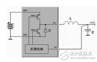
Figure 1 Buck topology
(2) In the steady state process, the following conditions must be valid:
(3) Equation 3 means that the coil current IL at the beginning of each clock cycle must be equal to the coil current IL at the end of each clock cycle (otherwise the system is not steady). From this condition, we can derive the duty cycle formula of the buck converter.
(4) Equation 4 means that the total amount of electricity generated by the coil must be equal to the total amount of power consumed by the load, assuming all switches and RDSOn losses are ignored.
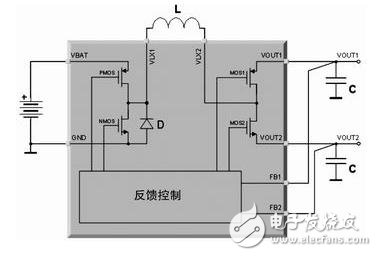
Figure 2 coil current waveform
For a dual output topology, in the STw4141 regulator, the current generated by the coil is distributed to two outputs, and the load current obtained from the two output ports can (actually always) be completely uncorrelated. Therefore, the steady-state condition of Equation 4 must be rewritten as:
(6) where Iload1 is the current drawn by the load from output 1, and Iload2 is the current drawn by the load from output 2.
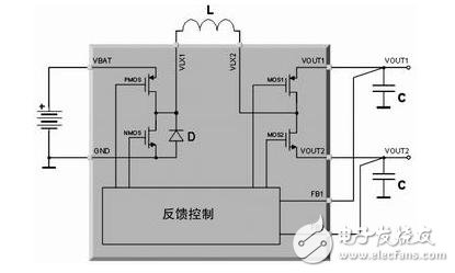
Figure 3 STw4141 topology
In order to distribute the power according to Equation 6, the system needs to add two switches MOS1 and MOS2, as shown in Figure 3. When MOS1 is turned on, the amount of electricity stored in the coil is transferred to output 1. When MOS2 is turned on, the amount of charge stored in the coil is transferred to the output 2.MOS1 and MOS2 to resemble the 1/T frequency of PMOS and NMOS. Inverting switch, and duty cycle D2. Different from PMOS and NMOS D1. It can be said that duty cycle D1 is the standard for measuring the total energy that the system can transmit, while duty cycle D2 is the measurement between the two outputs. The standard of total electrical energy. The most important factor to note is that the system requires only one coil.
Figure 4 is a waveform of a dual output topology coil current. Unlike traditional buck converters, the dual output topology has three main phases: (Vbat-Vout2)/L rising slope; -Vout2/L falling slope; -Vout1/L falling slope.
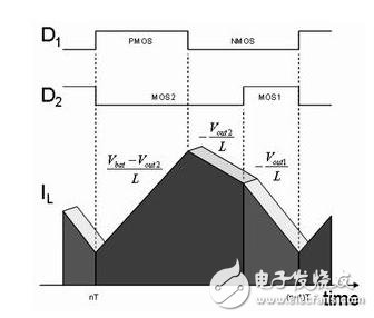
Figure 4 coil current waveform
performance
Measures to improve efficiency include synchronous rectification, pulse-frequency modulation PFM mode, minimizing RDSOn power consumption, and advanced internal enable/disable strategies.
Synchronous rectification is used to reduce the power dissipation caused by the forward voltage of diode D (see Figure 1). During the second cycle, the NMOS transistor is shorted to diode D, resulting in reduced power consumption.
(7) The current in the coil may be reversed, which is a known shortcoming of synchronous rectification technology, which leads to an increase in power consumption. STw4141 solves this problem by turning off the NMOS transistor when IL=0, preventing current backflow in the coil. The STw4141's synchronous rectification method greatly improves efficiency under moderate load conditions.
When the load is extremely low, the efficiency is further improved by entering the PFM mode. In PFM mode, the power conversion is no longer synchronized with the built-in oscillator, but instead delivers power to the output as needed. Minimizing the power stage commutation frequency, coupled with disabling the useless internal oscillator in PFM mode, makes the STw4141 more power efficient, as shown in Figure 5. The STw4141 automatically selects the mode for optimal efficiency without user intervention.
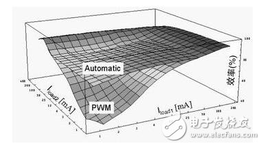
Figure 5 efficiency characteristics
The way the PFM mode is used depends on the application of the chip. Because power conversion is asynchronous in PFM mode, electromagnetic radiation can produce spectral noise at sensitive frequencies. If such a constraint exists, there are two ways to configure it: the PFM mode is completely disabled; the user can override the automatic switch to force the mode into operation. Designers can use the overlay function to design a power system that is both energy efficient and spectrally no interference. In standby mode, an application processor that performs 95% of the process time-critical is an example of such a system, since the processor must also save data in standby mode, so it can be powered in standby mode. Within a few microseconds before the processor wake-up signal is received, the chip is forced into Pulse Width Modulation (PWM) mode and remains in this mode until the advanced system returns the processor to sleep mode. Additional features
Spectral interference is a problem that may exist in sensitive applications, and the industry has been studying this phenomenon. A research report shows that in practical applications, certain frequencies should be avoided, while other frequencies do not affect the entire system. The frequency of the STw4141 internal oscillator (taking into account its spectrum) may be in the harmful band. For this reason, a phase-locked loop (PLL) is provided that allows the user to synchronize the internal oscillator over a wide frequency range outside the unwanted band. The phase-locked loop also suppresses the spectrum of the built-in oscillator, allowing the STw4141 to synchronize with other components of the system.
The high voltage output Vout1 is typically used for the I/O pin structure (VIO) and the low voltage output Vout2 is typically used for the digital core (VCORE). To support multiple processors, a wide range of VIO voltages and VCORE voltage ranges from 1.0V to 1.8V are available. The user can set the output voltage through a dedicated pin. This feature is useful in applications that save power by reducing the application processor supply voltage into sleep mode. VCORE control can be used with the mode control (PWM/PFM) mentioned above, but there is a big difference between the two: VCORE control reduces the power consumption of the application processor, while mode control reduces the power consumption of the chip. Both features reduce the power consumption of the entire application.
In addition, the STw4141 features peak current limiting and thermal protection. The peak current limiting function not only protects the chip itself, but also limits the current drawn by the chip from the battery. Due to the internal series resistance of the battery, excessive current drawn from the battery may cause a large change in the battery voltage.
typical application
The most important factor that causes the STw4141 to reduce size and cost is that it requires only one external coil, while a normal power supply requires two. Figure 6 shows the recommended external component layout, which is a 7 x 8 mm board designed for a complete application. In this design, the coil is the largest component, and the board space is also the component. Secondly, the BGA package also plays an important role in saving board space.
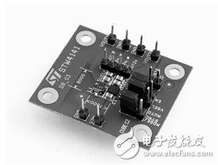
Figure 6 STw4141 application board
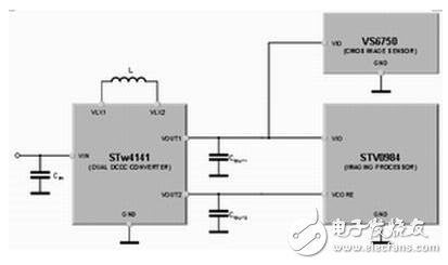
Figure 7 typical application
The commonality of the STn8810 multimedia application processor (NOMADIK) and the STV0984 + VS6750 image processor and the 2 megapixel CMOS image sensor is that the digital core voltage (VCORE) is different from the I/O pin supply voltage (VIO). Figure 7 is a circuit diagram of a CMOS camera application. The VCORE voltage (1.2 V) is supplied to the digital core STV0984, and the VIO voltage (1.8V) is used to supply the I/O structure of the VS6750 and STV0984. This layout design makes the application board extremely compact.
Conclusion
The product is comparable in efficiency to two independent switching power supplies and is sized to two independent LDO power supplies. Therefore, it is possible to replace the linear power supply in a portable device or to reduce the physical size and cost of the switching regulator.
Nxairs Air Insulated Switchgear
Nxairs Air Insulated Switchgear,Gas Insulated Switchgear,Pole Mounted Switchgear,Power Electric Switchgear
Shandong Shunkai electrical equipment co., LTD. , https://www.chinasdsk.com