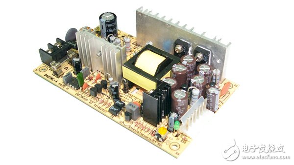
In the switching power supply design, the physical design of the PCB board is the last link. If the design method is improper, the PCB may radiate too much electromagnetic interference, causing the power supply to work unstable. The following points are analyzed for the matters needing attention in each step:
From schematic to PCB design flow
Establish component parameters - "Input Principle Netlist -" Design Parameter Settings - "Manual Layout -" Manual Wiring - "Verification Design - "Review -" CAM output.
Component layout
Practice has proved that even if the schematic design of the circuit is correct and the printed circuit board is not properly designed, it will adversely affect the reliability of the electronic device. For example, if the two thin parallel lines of the printed board are close together, the delay of the signal waveform will be formed, and the reflection noise will be formed at the end of the transmission line; the interference caused by the inconsistency of the power supply and the ground line will cause the product to be Performance is degraded, so when designing a printed circuit board, care should be taken to use the correct method. Each switching power supply has four current loops:
(1) Power switch AC circuit
(2) Output rectifier AC circuit
(3) Input signal source current loop
(4) Output load current loop input loop
The input capacitor is charged by an approximately DC current. The filter capacitor acts primarily as a broadband energy storage; similarly, the output filter capacitor is also used to store the high frequency energy from the output rectifier while eliminating the DC energy of the output load loop. Therefore, the terminals of the input and output filter capacitors are very important. The input and output current loops should be connected only from the terminals of the filter capacitor to the power supply; if the connection between the input/output loop and the power switch/rectifier loop cannot be connected to the capacitor The terminals are directly connected and the AC energy is radiated from the input or output filter capacitors to the environment.
The AC circuit of the power switch AC circuit and the rectifier contains high amplitude trapezoidal currents. The harmonic components of these currents are very high, and the frequency is much larger than the fundamental frequency of the switch. The peak amplitude can be up to 5 times the amplitude of the continuous input/output DC current. The transition time is usually It is about 50 ns.
These two loops are the most susceptible to electromagnetic interference, so these AC loops must be placed before other traces in the power supply. The three main components of each loop are filter capacitors, power switches or rectifiers, inductors or transformers. Place them adjacent to each other and adjust the component position so that the current path between them is as short as possible. The best way to establish a switching power supply layout is similar to its electrical design. The best design flow is as follows:
Place transformer
Designing the power switch current loop
Design output rectifier current loop
Control circuit connected to the AC power circuit
Designing the input current source loop and input filter design The output load loop and output filter follow the following principles when laying out all the components of the circuit according to the functional unit of the circuit:
(1) First consider the size of the PC B. When the size of PC B is too large, the printed lines are long, the impedance is increased, the noise resistance is reduced, and the cost is also increased; if the size is too small, the heat dissipation is not good, and the adjacent lines are susceptible to interference. The optimal shape of the board is rectangular, with an aspect ratio of 3: 2 or 4: 3, and the components located at the edge of the board are generally not less than 2 mm from the edge of the board.
(2) Consider the future soldering when placing the device, not too dense.
(3) Centering around the core components of each functional circuit, it is laid out around it. Components should be evenly, neatly and compactly placed on PC B to minimize and shorten leads and connections between components. The decoupling capacitors should be as close as possible to the VCC of the device.
(4) For circuits operating at high frequencies, the distribution parameters between components should be considered. In general, the circuit should be arranged in parallel as much as possible. In this way, it is not only beautiful, but also easy to weld and easy to mass produce.
(5) Arrange the position of each functional circuit unit according to the flow of the circuit, so that the layout facilitates signal circulation and keeps the signal as consistent as possible.
(6) The first principle of layout is to ensure the wiring rate of the wiring. Pay attention to the connection of the flying line when moving the device, and put the devices with the connection relationship together.
(7) Reduce the loop area as much as possible to suppress radiated interference from the switching power supply.
parameter settings
Adjacent conductor spacing must meet electrical safety requirements, and spacing should be as wide as possible for ease of operation and production. The minimum spacing should be at least suitable for the voltage to withstand. When the wiring density is low, the spacing of the signal lines can be appropriately increased. The signal lines with high and low levels should be as short as possible and the spacing should be increased. Set the trace spacing to 8 mils.
The distance from the edge of the pad to the edge of the board is greater than 1m, which avoids pad defects during processing. When the traces connected to the pads are thinner, the connection between the pads and the traces is designed to be drop-shaped. This has the advantage that the pads are not easy to peel, but the traces are not easily disconnected from the pads.
BLPS laser safety protective device is designed for personal safety used on hydraulic bender.
The dynamic test technology it used has passed the Type 4 functional safety assessment by TUV, and get the national invention patent. The product reaches the advanced technological level of similar products.
BLPS laser safety device provides protection zone near the die tip of the bender to protect fingers and arms of the operator in close to the upper mold die tip. It is the most effective solution so far to preserves the safety and productivity of the bender.
Press Brake Protection,Laser Guarding Device,Press Brake Guarding Systems,Press Brake Guarding
Jining KeLi Photoelectronic Industrial Co.,Ltd , https://www.sdkelien.com