In the past car audio system design, the highest clock frequency on a PCB is already high at 30 ~ 50MHz, but now the clock frequency of most PCBs exceeds 100MHz, and some even reach the order of GHz. For this reason, the traditional serial design method driven by netlist can no longer meet today's design requirements. Now we must adopt an updated design concept and design method, that is, the serial design process driven by netlist will be changed to the whole Design a parallel process for each link to be considered in parallel. In other words, the design requirements and constraints that were only considered in the PCB layout and wiring stage in the past were changed to give enough attention and evaluation in the schematic design stage. At the early stage of the design, the selection of key devices was analyzed and the key network cables were conceived. Topology, termination matching network settings, and full consideration of the PCB stack-up structure before wiring starts to reduce crosstalk between signals, ensure power integrity and timing and other factors.
This article mainly introduces the high-speed DDR200 used in the car audio navigation system. Under the guidance of the basic theory of high-speed circuits and professional design experience, the PCB design method to ensure signal integrity.
1 What is DDR and its basic working principle
DDR SDRAM is commonly known as DDR. DDR SDRAM is double-rate synchronous dynamic random access memory.
DDR memory is developed on the basis of SDRAM memory. SDRAM only transmits data once in a clock cycle, it transmits data during the rising period of the clock; while DDR memory transmits data twice during a clock cycle, it can transmit data once during the rising period and falling period , So called double rate synchronous dynamic random access memory. DDR memory can achieve double the data transfer rate at the same bus frequency as SDRAM.
As shown in Figure 1 and Figure 2 below, DDR SDRAM has two more signals than SDRAM: CLK # and DQS.
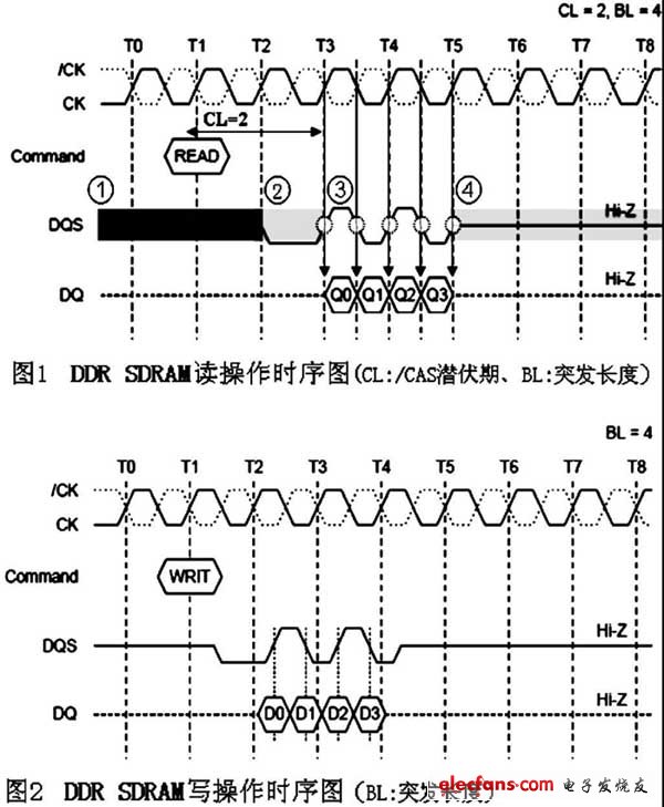
CLK # is opposite to the normal CLK clock phase, forming a differential clock signal. The data transmission is performed at the intersection of CLK and CLK #, that is, data is triggered on both the rising and falling edges of CLK (which is exactly the rising edge of CLK # at this time), thereby achieving double-rate transmission.
DQS (DQ STrobe, data selection pulse) is an important function in DDRSDRAM. It is mainly used to accurately distinguish each transmission cycle within a clock cycle, and uses DQS to read the corresponding data DQ at the receiving end.
DQS is valid on both rising and falling edges and is generated at the same time as the data signal. DQS and DQ are two-way transmission of three-state signals. During the read operation, the edge of the DQS signal is aligned in timing with the edge of the DQ signal, while during the write operation, the edge of the DQS signal is aligned in timing with the center of the DQ signal.
The following uses Figure 1-DDR SDRAM read operation timing diagram as an example to illustrate the control principle of DQS:
â‘ DQS is at a high impedance level when there is no data output.
â‘¡ After receiving the READ command, the DQS signal becomes low impedance, and it is one cycle ahead of the data output time.
â‘¢ The DQS signal is generated at the intersection of CLK and CLK # at the same time as the data signal, and the frequency is the same as CLK.
â‘£ The DQS signal continues until the burst of the read pulse is completed, and then returns to the high impedance level again.
2 Basic specifications
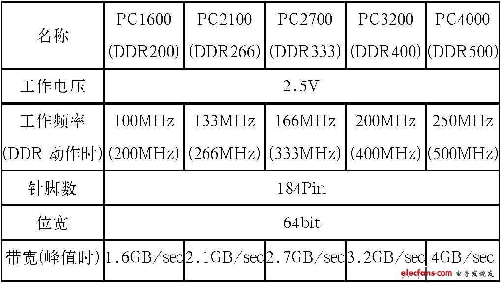
The basic specifications of DDR SDRAM (Table 1).
Table 1 Basic specifications of DDR SDRAM
3 PCB design method of DDR200
The following uses the DDR200 used in the car audio navigation system as an example, the PCB design method from the aspects of PCB stack structure selection, wiring topology, crosstalk, power integrity and timing.
3.1 Selection of PCB stack structure
The laminated structure of the circuit board directly determines the signal transmission speed and delay time in each conductor layer. According to circuit configuration and structural limitations, combined with EMI requirements such as high-speed signals and power supply return paths, it is very important to determine the stack structure and the wiring layer of important signals in the early stage of design. The stacked structure of this example and the wiring layers of important signals are shown in Figure 3.
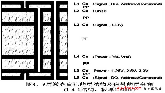
Depending on the plate, the thickness of the conductor copper, the thickness of each insulation layer and the dielectric constant will also be different, resulting in differences in the characteristic impedance Zo and the transmission delay Tpd of the high-speed signal transmission line.
When the dielectric constant of the insulating medium in the plate is εr = 4.0, the thickness of the insulating layer PP1 = 60μm, PP2 = 200μm, PP3 = 800μm, the thickness of the conductor copper is 35μm, and the line width W = 100μm, the signal is transmitted on the surface layer (L1, L6) Delay Tpd ≒ 140ps, characteristic impedance Zo ≒ 56Ω, transmission delay Tpd ≒ 170ps in inner layer L3 wiring, characteristic impedance Zo ≒ 84Ω.
Young LivingAlarm Clock Oil Aroma Diffuser Manufacturers and Suppliers in China
The Aroma Oil Diffuser with Alarm Clock is the perfect way to vaporise in Essence Pure Essential Oils. The micro-fine cool mist disperses the essential oil particles into the air in their purest form to promote physical and emotional health when inhaled. Meanwhile, the latest ultra-sonic wave technology purifies the air of unwanted germs and acts as a humidifier without condensation.
Additional features include:
- Alarm Clock Aroma Diffuser with Alarm clock setting
- Alarm Clock Diffuser with LED time display
- Young Living Oil Diffuser with Touch control for easy use
- Aroma Diffuser with LED lighting options featuring 7 colours
Alarm Clock Diffuser
Aroma Oil Diffuser,Alarm Clock Aroma Diffuser,Young Living Oil Diffuser,Alarm Clock Diffuser
Shenzhen Dituo Electronic Co.,Ltd. , https://www.sz-dituo.com