After the merger between AWR and American National Instruments is completed, AWR's ambition to advance into the Asian RF design tool market is expected to be further realized through the improvement of its hardware and software integration capabilities; at the same time, Agilent has also joined hands with TSMC To create an RF design and development kit, the future battle between the two major EDA tool suppliers in the Asian market is inevitable.
Due to the increasing importance of wireless networking design in mobile networking devices, how to solve the radio frequency (RF) / high frequency design challenges has become a difficult problem for the wireless communication industry to overcome. Therefore, electronic design automation (EDA) tools that can further optimize the design process and accelerate the time-to-market have become an obvious subject of competition in the industry. Especially in the Asian market where hundreds of mobile device products are contending, the demand for high-efficiency design tools is even more intense, which has also prompted relevant EDA tool suppliers to lock in this market opportunity and have begun to arrange card positions.
Soft and hard integration adds momentum to AWR Rio Tinto's Asian market
Aiming at the trend of rising demand for wireless communication EDA tools in Asia, AWR, who is eager to enter the market, is expected to publish a new version of the RF / microwave design platform Microwave Office 10.0 in October, and introduce the 3D FEM EM function early next year In the future, through the development of hardware and software after the merger with NI, it will open up the Asian wireless communication design market, and then differentiate itself from the market leader Agilent (Agilent).

Figure 1 Sherry Hess (left), vice president of AWR marketing, said that for 4G demand, AWR will use the smooth and complete EDA tools to attack the Taiwan, Japan, South Korea, and China markets. On the right is Xu Dongcai, Deputy General Manager of AWR Taiwan Agent Tsukuba Technology Marketing.
AWR marketing vice president Sherry Hess (left in Figure 1) analyzed that the combination of NI and AWR will make the two sides more prominent in the market. In addition to NI's ability to improve the software capabilities and win the leader in the field of RF testing, AWR Through NI's solid foundation in Asia, such as Shanghai, Beijing, Taiwan, South Korea's R & D and design centers, sales channels and partners, we can further expand its RF design tools' share in the Asian market.
In response to the development of AWR design tools, AWR Asia Pacific Manager Liang Zhiwei pointed out that AWR's main product Microwave Office platform will be updated to version 10.0 in October, mainly for RF and single crystal microwave integrated circuit (MMIC) product design and introducing two major innovations Features. First of all, the X-Models function is customized for users, allowing engineers to set the X-axis change parameters, and then output various design frameworks, gradually depicting designs that meet their product needs, to speed up the time to market. Secondly, the simulation yield and optimization (EM Yield and OpTImizaTIon) function, through the software's integrated diagram and layout (Layout), is faster and more complete than previous versions of the output design model to help identify design defects .
It is worth mentioning that the Microwave Office platform will introduce 3D electromagnetic simulation function early next year, which adds Z-axis variables to produce 3D models close to the physical design, allowing engineers to obtain complete design information, not only to list the structural defects of the product. Extensively, it also saves a lot of development time.
In fact, AWR is extremely influential in the US, Europe and other markets, and its Microwave Office design platform for RF / microwave products has a market share of up to 50%. However, AWR only gradually expanded the Asian market in 2005. So far, its market share is only about 10%, far behind that of competitors Genesys RF / microwave design software. Therefore, Hess emphasized that AWR has been intensively expanding its layout, in addition to integrating with the hardware and software of NI, and will replicate the successful development experience in the United States and Europe, continue to strengthen its design tools, by designing the platform in the second half and next year The newly added diversified features attracted the attention of engineers, and then divided the Asian market share of Agilent.
Hess further explained that RF design is becoming more and more complicated, and the market competition is fierce, and the product launch time is continuously compressed. Therefore, only with solid EDA tools can you have good design and production capabilities, and you will not be overwhelmed by market trends. While the Asian wireless communication market is taking off, although AWR's footsteps in Asia are slower, with its rich experience and focus on EDA tools, it will be able to provide solutions that meet all customer needs; and AWR has always been The design tools are known for their simplicity and convenience, making it easy for users to get started. It is an unparalleled advantage of competitors. I believe the market will be happy to accept this new choice.
NI founder and CEO James Truchard also said that AWR specializes in RF-related technologies and can extend the NI platform into RF design; combining the expertise of both parties, they can also jointly strengthen core software such as NI LabVIEW, AWR Microwave Office, AWR Visual System Simulator, and RF test hardware platform, make customers' product design more efficient and shorten the time to market.
AWR CEO Dane Collins believes that there is a clear complementarity between the products and customers of the two companies. NI's testing and prototyping platform for RF systems is important, and AWR's RF circuit and system software design tools will complement each other to provide better services.
Drive into the TSMC design kit Agilent full force
On the other hand, Agilent, which has a strong position in RF design tools in the Asian market, has also announced that its SystemVue, GoldenGate and Momentum RF IC design solutions will be included in TSMC ’s version 3.0 65nm 60GHz RF reference design kit to further integrate RF systems, The design and analysis at the subsystem and component level are integrated into the complete design process and continue to expand the layout of RF design tools in the Asian market.
Zhang Zhiming, chairman of Agilent Technologies Taiwan and general manager of the electronic measurement business group, said that until recently, customers had to establish their own when developing 60GHz complementary metal oxide semiconductor (CMOS) wireless ultra-high-speed links (Gigabit Link) or radar ICs. And maintenance of millimeter wave CMOS process design kit (PDK) is quite time-consuming and laborious. TSMC and Agilent integrate all resources for customers by providing certified millimeter-wave PDK, including 60GHz CMOS reference design and teaching courses, as well as Agilent's complete millimeter-wave CMOS design solution for Cadence Virtuoso platform.
Suk Lee, director of TSMC's design infrastructure marketing, pointed out that TSMC's reference design kit was developed using Agilent's simulation and model building solutions. The kit provides simulation results related to silicon design, as well as simulation test rules for extracting S-parameter models of different interconnections, transmission lines and transformers. It also has process teaching to assist customers in designing high-frequency and high-bandwidth wireless ICs.
Suk Lee emphasized that Agilent plays an important role in RF and electromagnetic design tools in Asia, so it has become the best choice for TSMC when selecting partners for 60GHz reference design kits. After the technologies of both parties are combined, a complete simulation and model building solution that crosses the boundaries of systems, millimeter wave circuits and interconnected components is expected.
10 Layer PCB Stack Up thickness, Design and manufacturing
Usually, 10 layer PCB is HDI board, but some are not.
10 Layer PCB Stack Up And Design
Regardless of the number of layers constituting the circuit board design, pad spacing, clearance, trace widths, copper weights and drill hole sizes must be tailored to your contract manufacturer (CM). If your design requires multiple layers, you need to consider additional DFM specifications for signals through vias, power and ground wiring, and PCB stackup.
For 10-layer PCB Manufacturing, it is necessary to determine the number of layers, their arrangement or stacking, and the type of material. These choices require coordination between thickness constraints; material parameters; such as dielectric constant, thermal expansion coefficient and electrical strength; signal type isolation and drilling options. For PCB Assembly , wiring options and their impact on welding process are very important. The function of CM limits the choice of vertical aspect of design.
When your PCB needs six layers of routing, you should choose to use ten layers of PCB. Because ten-layer circuit boards usually have six signal layers and four planes. Of course, we do not recommend the design of more than six signal layers on the 10-layer circuit board. Ten layers are also the largest number of layers, which can be easily manufactured on 0.062 inch thick sheets. Occasionally you will see a 12-layer PCB made of 0.062 inch thick board, but there are not many manufacturers who can make 12-layer circuit boards. Just right, besides making 10-layer circuit boards, we also have very rich experience in manufacturing 12-layer circuit boards.
High layer count boards (10 +) require thin dielectrics (usually 0.006 or smaller on 0.062 thick plates), so they are automatically tightly coupled. After stacking and wiring properly, they can meet all our goals and have excellent EMC performance and signal integrity.
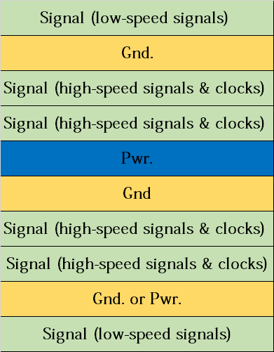
The reason why this stack has such good performance is the tight coupling between signal and return plane, the existence of high-speed shielding signal layer, multiple grounding layers, and tightly coupled power supply/grounding layer pairs in the center of circuit board.
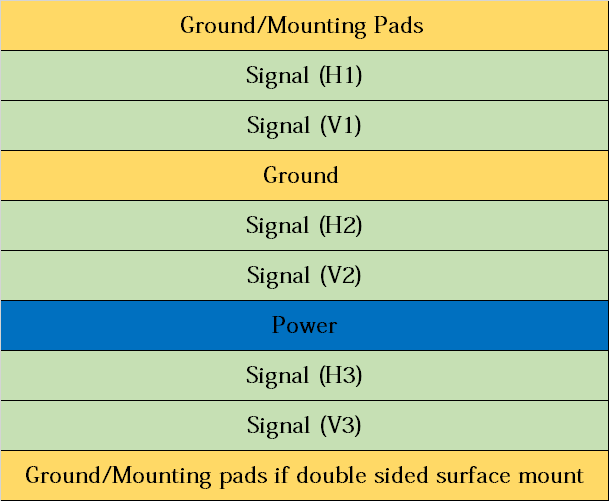
This 10-layer PCB stacking up method abandons closely spaced power/ground pairs. In return, it provides three signal routing layer pairs, shielded by the ground layer on the outer layer of the board, and isolated from each other through the internal power supply and the ground layer.
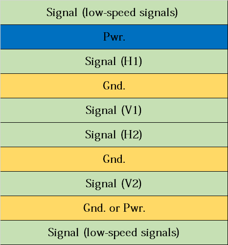
This 10-layer PCB stackup allows the routing of orthogonal signals near the same plane, but in the process, the closely spaced power/ground plane must also be abandoned.
In addition, we list some other stacking methods of 10-layer circuit boards for your reference.
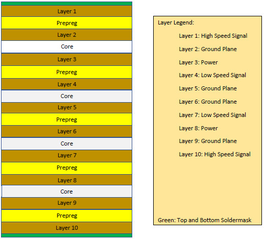
10 Layer PCB Thickness
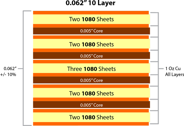
0.062''10 Layer PCB Stackup thickness
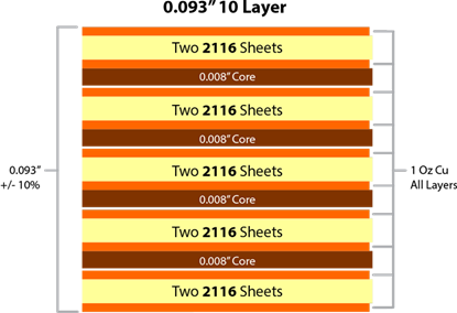
0.093'' 10 Layer PCB Stack UP thickness
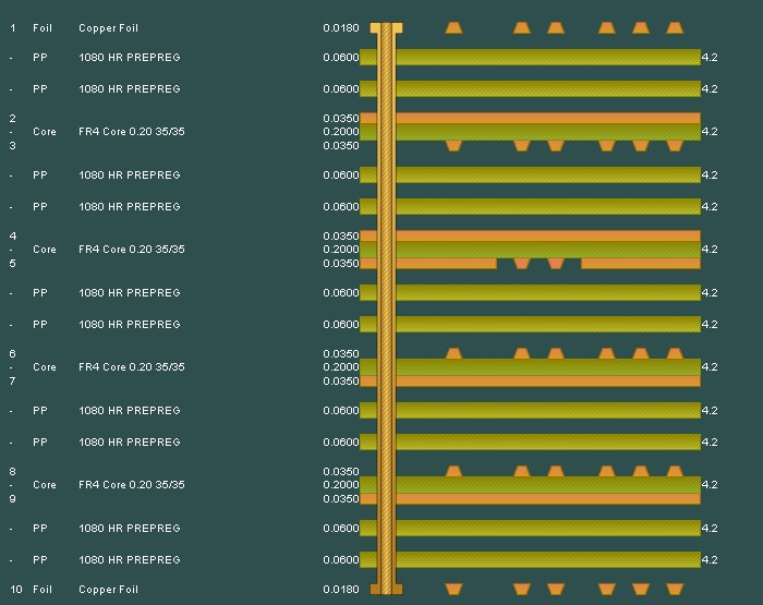
10 Layer Stackup - 1.6mm thickness
layer order
layer name
material type
material description
dielectric constant
thickness
copper weight
1
top
copper
signal
0.035mm
1 oz
7630
prepreg
4.7
0.2mm
2
inner 1
copper
plane
1 oz
core
4.6
0.2mm
3
inner 2
copper
plane
1 oz
2116
prepreg
4.5
0.12mm
4
inner 3
copper
plane
1 oz
core
4.6
0.2mm
5
inner 4
copper
plane
1 oz
2116
prepreg
4.5
0.12mm
6
inner 5
copper
plane
1 oz
core
4.6
0.2mm
7
inner 6
copper
plane
1 oz
2116
prepreg
4.5
0.12mm
8
inner 7
copper
plane
1 oz
2116
prepreg
4.6
0.2mm
9
inner 8
copper
plane
1 oz
7630
prepreg
4.7
0.2mm
10
bottom
copper
signal
0.035mm
1 oz
Final board thickness: 1.6mm±0.16mm
10 Layer PCB Application
With the rapid development of today's increasingly complex multi-layer PCB, machines and equipment in various industries - commerce, industry, medicine, government, Aerospace - continue to grow in terms of speed, capacity, compactness and ease of use.
8, 10 and 12 layers of multi-layer PCB are useful in many high-tech equipment and computer systems. In recent decades, the development of multi-layer Printed Circuit Boards has led to the rapid development of computer technology - from the previous Gigabit system to today's GHz machine.
Especially 10-layer PCB, which is widely used in the following industries: Preamplifier, Satellite Dish, GPS Tracking Devices, SAN Storage, AC Drives, GSM Signal Booster, Mobile Broadband Router, Inverter 220V, Memory Module, Automotive dashboards
Cheap 10 Layer PCB manufacturing services
For customized printed circuit boards, our 10-layer PCB offers the fastest turning time for the best price we can offer. For on-demand pricing and ordering of your next Printed Circuit Board project, you can contact our online customer support or send us an email to get 10-layer PCB quotation immediately.
10 Layer PCB
Printed Wire Board,Custom PCB Board,10 Layer PCB,10 Layer PCB Stackup
JingHongYi PCB (HK) Co., Limited , https://www.pcbjhy.com
