Design and hardware implementation of ultrashort wave band pulse generator
Overview: The method of generating pulses is considered from the frequency domain perspective. The filter is used to shape the unit impulse response to achieve the purpose of controlling the pulses within a fixed frequency spectrum. Simulation design and hardware implementation of the circuit through ADS and Protel. The test result shows that the output result of the pulse generator meets the expected requirements, and the measured result agrees well with the simulation result. The peak-to-peak value of the final output pulse is 1.17 V, and the tailing suppression is -12 dB, which has good symmetry, and the frequency spectrum is basically controlled between 30 and 40 MHz.
Using the concept of ultra-wideband to realize ultra-wideband communication in the ultra-short wave band can meet the requirements of anti-interference performance in complex electromagnetic environment. In order to combine ultra-wideband technology with existing ultra-short-wave communication equipment, it is essential to design a reasonable ultra-wideband RF front end.
Ultra-wideband in the form of pulse is defined as the ratio of the signal energy bandwidth to the center frequency is greater than 0.20 ~ 0.25, on this basis, this paper designed an energy bandwidth between 30 ~ 40 MHz, the center frequency is 35 MHz Broadband signals, because the relative bandwidth = (fH-fL) / [(fH + fL) / 2] = 0.28> 0.25, so such a signal meets the definition of ultra-wideband. At this stage, the hardware form for implementing ultra-wideband pulses is mainly to use the physical characteristics of special semiconductor devices or the reflection combination of microstrip lines to form a UWB signal that meets the requirements. The controllability of the spectral characteristics of this UWB signal is very poor, generally Determined by the properties of the semiconductor itself. Therefore, in order to accurately control the spectral characteristics of the pulse, the implementation of the pulse generator must start from the frequency domain of the signal.
On this basis, this paper considers a pulse generator based on a filter shaping network. The principle of this pulse generator is: the baseband square wave signal passes through a differential circuit to extract the rising and falling edges of the baseband pulse to obtain a unit impulse pulse, and then passes through a zero-bias amplifier circuit to filter out the falling edge and amplify On the rising edge, the amplified unit impulse pulse is pulse shaped through the filter shaping network to form a broadband signal with limited frequency domain, and finally amplified and transmitted. As long as the filter shaping network in the circuit is properly designed, different design requirements can be achieved.
l Schematic diagram design According to the above ideas, the block diagram of the pulse generator is shown in Figure 1.
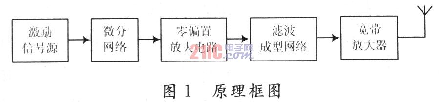
The excitation signal source is a square wave signal of TTL level, with a high level of 3.3 V and a low level of 0 V. But the rising edge time and falling edge time should not be too long, it should be around 1 ns. The design requires a pulse bandwidth of 10 MHz. In order to prevent cross-talk between codes, the repetition frequency of the signal source is controlled at 1.25 MHz. The differential network consists of capacitors and resistors. In fact, it is a high-pass circuit with a short time constant. Its function is to extract the rising and falling edges of the square wave signal to reduce the duty cycle of the signal. The zero-bias amplifier circuit amplifies the forward differential signal while filtering out the reverse differential signal formed by the falling edge. The filter shaping network shapes the differentially amplified signal to produce the required waveform shape and frequency spectrum, and finally the pulse is output to the radio frequency port through the broadband amplification circuit. The excitation signal source, differential network, and zero-bias amplifier circuit can be regarded as an ideal impulse generator.
2 Realization of specific circuit The design of the circuit is simulated using Agilent's ADS2006A. The ideal impulse generator is composed of an excitation signal source, a differential network, and a zero-bias amplifier circuit, as shown in Figure 2.

The excitation signal source is a square wave signal Vin with TTL level, the rising and falling edges are both 1 ns, and the excitation signal width is 400 ns. The differential network consists of a high-pass circuit whose RC time constant is much shorter than the input pulse duration. This circuit is used to change the square wave voltage applied to the input terminal into positive and negative peak voltage output. Because the output voltage represents the rate of change of the input voltage, this process of change is called differentiation. Two key points of the design of the differential circuit: τ << t plus / 10 to obtain a good impulse response; and a reasonable value of the resistor R to obtain a sufficiently large voltage amplitude. In this design, C1 = 3 pF, R = 120 Ω, time constant τ = RC = 3 × 10-12 × 120 = 3.6 ns.
The zero-bias amplifier network uses a single-stage transistor common-emitter amplifier circuit, and BJT uses infineon's BFP450. Because the amplifier circuit is to filter out negative pulses, the transistor must be operated at the critical point of the cut-off region and the amplification region. The steps to design a single-stage transistor amplifier circuit are static first and then dynamic. Through the ADS on the BFP450 DC operating point test to find a suitable static operating point. In the zero-bias amplifier circuit, R2 and R1 in the differential circuit together form a voltage-dividing DC path.
According to the data sheet of BFP450, the maximum base current IBB = 10 mA, the maximum collector junction voltage is VCE = 15 V, so the scanning range is: IBB = 20 ~ 100μA, the step is 10μA. VCE = 0 ~ 10 V, the step is O. 1 V. Import the Spice model of BFP450 into ADS to get the scanning result of static working point, as shown in Figure 3.
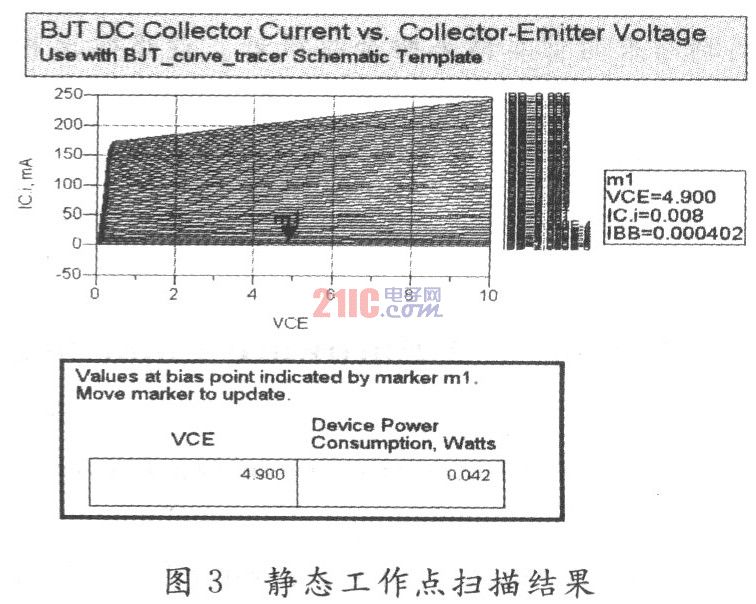
It can be seen from the scan results that for IBB <20μA, it can be considered that the transistor has entered the cut-off region. At the same time, when setting the static operating point, try to make the circuit have a larger linear amplification area, which is more conducive to the amplification of the pulse. So the selected test conditions are: VCE = 4 ~ 5V, step 0.1V. VCE = 500 ~ 600mV, step 20mV. Within this range, according to the formula:
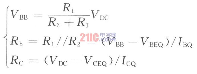
Derive R2 = 1 kΩ, R4 = 1 kΩ. Then bring the resistance back to the bias circuit, and the static operating point is IBB = 14.96 μA, Ic = 23.77 μA, VBE = 534.1 mV, VCE = 4.976 V. The output of each level of the ideal impulse shaping network is shown in Figure 4.
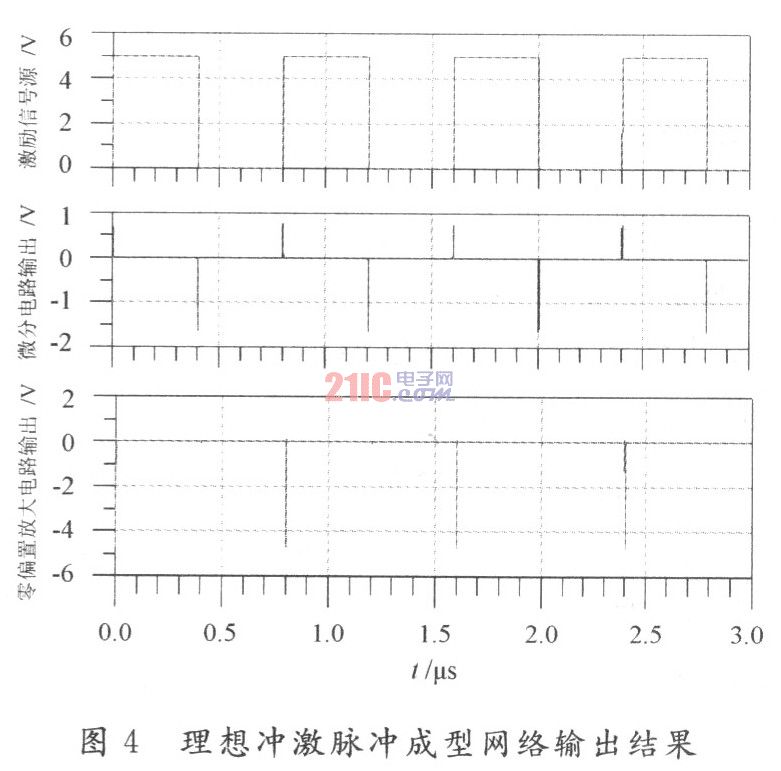
From the output results, the expected results are basically achieved, the forward differential signal is extracted, and inverted to 5 V, and the tailing oscillation is very small. The most important in the design scheme is the pulse shaping network, which determines the frequency range of the output pulse and the shape of the time domain. So use SmartComponentchart in ADS2006A for auxiliary design. The design specifications are: the filter type is a 5th order Chebyshev filter, the passband flatness is 0.5 dB, and the range is 30 to 40 MHz. The stopband attenuation is 50 dB, and the range is 10 MHz, 50 MHz. The input and output impedances are 50Ω. As shown in Figure 5.

The final link in the design is the broadband amplifier. What is adopted in this scheme is the common-shot negative feedback static operating point stabilization circuit. The emitter resistance Re and the coupling capacitance Ce are added on the basis of the zero-bias amplifier circuit, and the static operating point is stabilized by the negative feedback effect of Re. The criterion is: (1 + β) Re >> Rb. BJT still uses BFP450. According to the design method of the zero-bias amplifier circuit, the influence of Re is added to determine the static operating point as VCE = 2 V and VBE = 732.2 mV.
Because the single transistor is selected, rbb 'and Cμ are determined accordingly, so the gain-bandwidth product is also roughly determined, so the balance point between the gain and the bandwidth must be found during design. Second, the amplified spectral range of the broadband amplifier must be It is determined that between 30 and 40 MHz, no new frequency components can be introduced.
When designing the zero-bias amplifier circuit, the static operating point of the BFP450 has been determined, and negative feedback is introduced in this class of broadband amplifier circuit to stabilize the static operating point. Because it is a band-pass signal, the circuit is connected using a resistance-capacitance coupling method. The specific circuit is shown in Figure 6.
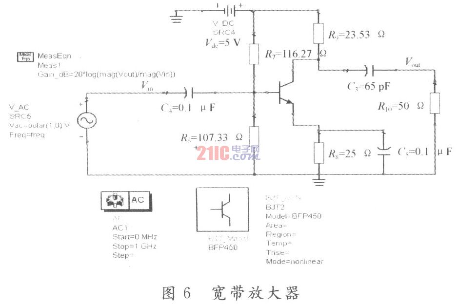
The frequency response of the single-tube amplifier circuit is:
(1) Lower cut-off frequency: 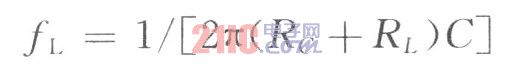
It has nothing to do with BJT's own parameters, only the time constant of the output loop.
(2) Upper cut-off frequency: 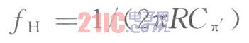
It is determined by the input circuit and the BJT's own parameters. Among them: is equivalent to the time constant of the input loop.
Knowing the BJT cutoff frequency fβ from the BFP datasheet, we can deduce, A. Because the output range of the filter forming network is 30-40MHz, the amplification range of the broadband amplifier is also controlled at this standard. According to the frequency response of the single-tube amplifier, the values ​​of resistance and capacitance can be calculated and converted to the nominal value according to the appropriate trade-offs. The gain of the broadband amplifier in the range of 30-40 MHz is: 21.36-22.56 dB.
The final circuit is shown in Figure 7.
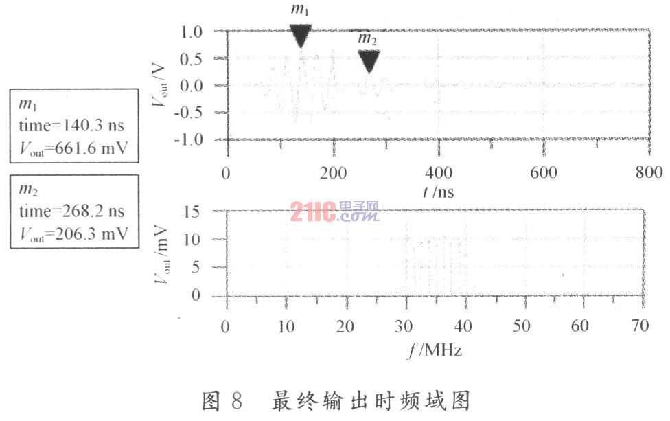
 Fig. 8 is a time-frequency domain diagram of the final output waveform of the pulse generator based on the filtering principle using ADS simulation. It can be seen from the figure that the peak-to-peak value of the final output pulse is -700 to 661.6 mV, and the tailing suppression is -12 dB. Note that the small amplitude oscillation after the main pulse is not caused by the circuit structure, but because of the limited frequency domain The signal must be an infinite oscillation in the time domain. In addition, the main pulse has good symmetry, and its frequency spectrum is basically controlled between 30 and 40 MHz. The repetition frequency of the pulse is determined according to the designed pulse width, in theory the maximum pulse repetition frequency. The simulation waveform is ideal and meets the expected requirements.
3 Manufacture and test of pulse generator The pulse generator circuit is made on FR4 epoxy glass fiber board, its dielectric constant is 9.6, thickness is 1.2 mm, input and output impedance is 50Ω, the whole circuit structure is compact ,small volume.
The input LO signal is 1. 25 MHz, a square wave with TTL level, and the output pulse waveform is measured using an Agilent 54855A, 6 GHz, 20 Gsa / s oscilloscope. The physical objects and test results of its pulse generator are shown in Figure 9.

The output pulse peak-to-peak value is 1.17V, the pulse width is 100ns, the pulse repetition is up to the maximum, the pulse center frequency is 35 MHz, the -10 dB bandwidth is 10 MHz, the passband flatness is 1 dB, and the stopband attenuation is 30 dB. It can be seen from the comparison with the simulation results that the tested pulse amplitude is smaller than the simulated pulse, and there is high-frequency signal interference at the front end of the pulse. Through analysis, it is known that high-frequency interference is the unit generated by the ideal impulse pulse generator The impulse pulse is caused by the crosstalk of the filter forming network to the analog ground, and the loop structure of the analog ground can be optimized in the next design to improve the pulse waveform. In general, the generated pulses have good symmetry, and all indicators have reached the expected requirements.
4 Conclusion In this paper, by considering the method of generating pulses from the frequency domain perspective, we have successfully designed a pulse generator that can be integrated on ultra-short wave communication equipment, thereby achieving ultra-wideband communication. This pulse generator has the advantages of compact structure, small size, low cost, and easy implementation. The test results are consistent with the simulation results. The outstanding advantage is that it can generate pulses in any frequency band by changing the parameters of the filter, and the maximum repetition frequency of the pulse breaks through the bottleneck of the traditional switching pulse generator limited by the characteristics of the switching device, and is only related to the pulse width generated. Connected to the post-stage power amplifier or transformer, it can realize high-speed and long-distance ultra-wideband communication.
A flourishing enterprise in this domain, engaged in presenting a wide range of Battery for UPS. The provided batteries are manufactured using different configurations, processes, battery backups, capacitates, and online options. Also, clients are facilitated to choose batteries from us having both online and manual systems. All installed batteries can bear the input power supply in-between 145V to 280V. The frequency rate of each battery is 50/60Hz. Moreover, entire battery systems provide the backup starting from 13minutes to 16 hours depending upon the usage.
100Ah 12V Solar Battery,12V Solar Battery,100Ah Solar Battery,Deep Cycle Solar Battery 12V 100Ah
Yangzhou Bright Solar Solutions Co., Ltd. , https://www.solarlights.pl