Direct frequency conversion receiver can realize multi-standard / multi-band reception
Mobile cellular operators have been eager to deploy a universal wireless infrastructure that can be field programmable to provide a variety of mobile services. Ultimately, the wireless infrastructure deployed in areas with relatively high cellular traffic needs to provide dynamic flexibility and enable RF hardware to adapt to changing signal conditions. Multi-standard / multi-band RF design can help solve the above problems by providing equipment assignments that can be easily customized to meet deployment needs. Compared with traditional receivers, advanced direct conversion provides a competitive solution for field-programmable RF design, saves costs, and has potential performance advantages. In addition, when using a single hardware solution to solve multi-band reception, the direct conversion architecture provides greater freedom. This is a more cost-effective solution that is making high-performance multi-standard / multi-band RF designs a reality. This article will discuss the performance and advantages of direct conversion receivers in 3G and 4G cellular applications.
High-performance direct conversion signal chain
The direct conversion receiver directly demodulates the radio frequency modulated carrier to the baseband frequency that can directly detect the signal and recover the transmitted information. The direct conversion architecture was first invented in 1932 to replace superheterodyne receivers. Since the intermediate frequency level is omitted, the number of components is also reduced, making it an attractive solution. By eliminating all the intermediate frequency stages and directly converting the signal to zero intermediate frequency, the mirroring problem in the superheterodyne architecture is eliminated. However, the direct conversion architecture also has some challenges, including local oscillator leakage, DC offset, and large distortion, which make the actual implementation difficult. However, recent advances in integrated radio frequency circuit technology have made traditional direct conversion (zero beat) architectures available for broadband high-performance receiver applications.
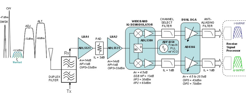
Figure 1: Architecture of a wideband direct conversion receiver.
Figure 1 shows the architecture of a wideband direct conversion receiver. In the signal chain, some key device indicators have been marked. The receiver signal path starts from the antenna port connected to a duplexer. Duplexers are commonly used in frequency division duplex (FDD) systems, such as W-CDMA and certain versions of WiMAX. The duplex filter network ensures that the transmitter does not generate too much harmful energy outside the licensed frequency band, and at the same time helps to suppress any out-of-band harmful signals introduced by the receiver input overdrive. Usually, after several stages of low noise amplifiers, there will be additional frequency band optional filtering and attenuation / matching network, the purpose is to optimize the receiving performance in the useful frequency range. The several levels of LNA in the figure provide excellent broadband performance, and also use an external tuning network to improve narrowband performance. When the receiver needs to solve a very wide frequency band reception, it may be necessary to use a switch matrix to configure the antenna network and LNA front-end optimized for some specific frequency bands. After the low noise front end, the IQ demodulator is used to down-convert the useful carrier frequency to the baseband frequency. A local oscillator signal with the same carrier frequency as the useful signal is added to the I / Q mixer at the baseband I / Q output port. , The sum frequency and the difference frequency are generated, and the low-pass filter suppresses the sum frequency, and only the difference frequency is allowed to pass. For zero-IF, the difference frequency is the baseband envelope of the useful signal. Using variable gain amplification is beneficial to quantify the amplitude of the filtered baseband I / Q signal. With VGA, the I / Q signal level can be adjusted to the optimal level required by the analog-to-digital converter. Generally, additional filtering is required before the ADC to ensure that high-frequency noise and possible leakage or interference are not aliased into the useful signal analysis bandwidth.
Receiver dynamic range
The receiver uses high-performance radio frequency integrated circuits that can provide wide-band coverage and instantaneous large dynamic range. The instantaneous dynamic range is a key indicator for all receivers used in a multi-carrier application environment, because here adjacent to the useful signal may be some strong interference signals with high power levels. Two-tone SFDR enables system designers to make more accurate predictions of nonlinear characteristics. The usual practice is to use single-tone or double-tone interference signals to test the receiver's ability to recover under strong signal blocking conditions. By studying the nonlinear characteristics of the receiver under two-tone excitation, various intercept points can be calculated, which is helpful for quantifying the receiver and modeling distortion performance and total dynamic range.
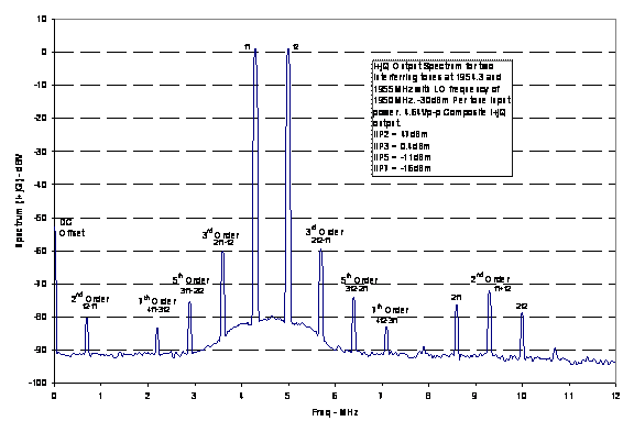
Figure 2: The two-tone intermodulation performance of the receiver shown in Figure 1.
Figure 2 shows the I + jQ output spectrum of the receiver when there are two continuous wave strong interferences near the frequency of the desired signal. In this test example, the input signal level added is –30dBm. This represents a more stringent blocking scenario than the required blocking test conditions in any specified 3G and 4G cellular systems. When sampling signals at or near baseband frequencies, the distortion caused by 2nd, 3rd, 4th, and even 5th and 7th harmonics will affect performance under large signal input conditions. In particular, the non-linear characteristics of the I / Q demodulator are particularly demanding to ensure that the intermodulation terms generated from the wanted signal and the unwanted signal will not degrade the useful signal of interest. Unlike the third-order intercept point (IP3), which is a common distortion in the design of most narrow-band IF sampling receivers, it is also important to focus on the distortion terms caused by even and odd nonlinearities. This type of nonlinearity is usually quantified with IP2, IP4, and IP5. In general, to ensure robust and reliable operation, it is important to evaluate all spurious signals that enter the receiver analysis bandwidth under the worst input conditions. Under such severe blocking conditions, intermodulation products generated by higher-order nonlinearities will fall into the frequency band and reduce the sensitivity of the receiver. The key non-linear items are marked in Figure 2. Please note how close several odd-numbered items are to the input fundamental frequency. This helps explain how close interfering signals will cause intermodulation products that fall within the useful signal band. When a direct conversion architecture is used, the difference frequency of the interfering signal (f2–f1)-the product of the limited 2nd-order nonlinearity of the receiver, will also fall within the frequency band of the useful signal.
ADIsimRF? Is ADI's free online signal chain calculator, which can be used to model the dynamic noise and distortion characteristics of the receiver under various test conditions. The nonlinear intercept point characteristics can be modeled and tested up to the 7th-order nonlinear term, and can be compared with the cascade intercept point predicted by ADIsimR. By evaluating the nonlinear characteristics of a single device and the entire cascade, the entire receive link can be better optimized to achieve the highest instantaneous dynamic range performance. The noise figure of a high-sensitivity receiver using this scheme is less than 2dB, and when applying the single-tone and two-tone interference levels specified in the W-CDMA specification (ETSI EN 302 217-2-2 V1.2.3 (2007-09)) , The desensitization of the receiver is less than 1dB.
Any local oscillator signal that leaks into the RF input port will be transmitted back to the receiver and form a self-mixing with the local oscillator signal. Self-mixing results in the squared term of the local oscillator signal, which will generate second harmonics. Although the high frequency generated by self-mixing can be greatly attenuated by low-pass filtering, DC falls into the frequency band of the direct mixing receiver. Note the DC term in Figure 2.
DC offset calibration and correction methods are usually required in baseband sampling systems. The residual DC offset is equivalent to the interference signal within the signal analysis bandwidth. There are several techniques that can reduce this effect, including DC tracking cancellation, baseband AC coupling, or a simple method—that is, by selecting devices with excellent DC characteristics (including higher even-order distortion characteristics).
Non-ideal quadrature and image rejection
I / Q amplitude and phase mismatch will cause a decrease in signal-to-noise performance. In an ideal I / Q demodulator, the phase relationship between the I and Q vectors of the baseband I / Q signal is 90 degrees, which is called ideal quadrature. Under ideal conditions, the identification of symbols in the digital domain can be easily achieved through instantaneous I / Q vector trajectories. However, when there is an I / Q mismatch in the system, the I / Q symbol vector will have amplitude and phase errors, which will reduce the signal-to-noise ratio of the recovered signal. The static error of I / Q can be eliminated by digital technology. It is very important to study the relationship between the effective image rejection of the direct conversion receiver and the amount of signal level and offset carrier frequency. Correctly understanding the impact of the receiver's single tone I / Q mismatch will help simplify the interpretation of the measured performance when a modulated signal is added.
Modulation error ratio performance
Modulation error ratio (MER) is a method used to measure the modulation accuracy of a digital transmitter or receiver. In an ideal linear and noise-free system, all I / Q symbols of the signal received by the receiver will be mapped to the exact position of the signal space constellation, and various non-ideal types in the design (such as amplitude imbalance, noise floor And the phase imbalance) will cause the measured symbol vector to deviate from its ideal position. The direct conversion receiver gives the MER performance level that various modulation schemes should emulate.
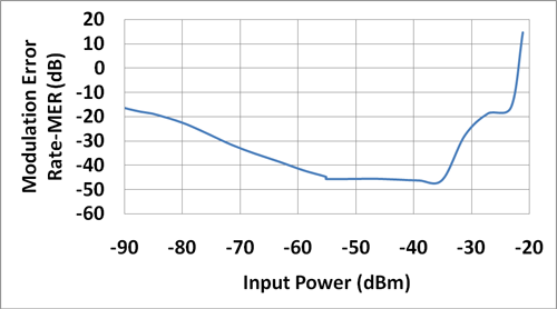
Figure 3: MER of 10MHz OFDMA WiMAX signal versus RF input power.
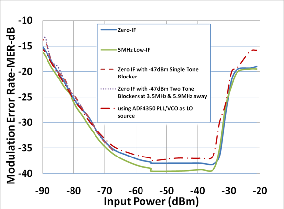
Figure 4: Relationship between MER of WCDMA signal and RF input power under zero-IF, low-IF, and blocking interference conditions.
Figures 3 and 4 plot the MER performance at different power levels for 10MHz wide OFDM, WiMAX, and WCDMA signals, respectively. Generally, the receiver has three factors that significantly limit the MER for the received input signal power. When the signal is strong, the distortion component falling into the band due to the receiver nonlinearity will greatly reduce the MER. When the signal level is medium, the receiver works in a linear state, and the signal is far greater than any noise contribution. At this time, the MER reaches its optimal value. At this time, the main control factors include the orthogonal accuracy of the demodulator, the filter network, and the Variable gain amplifier (VGA), and accuracy of test equipment. As the signal level continues to decrease, noise becomes the main factor, and the MER performance will decrease by dB with the signal level. At low signal levels, noise is the main limiting factor, and MER in decibels will be proportional to SNR.
Careful observation of Figure 4 reveals the recovery performance of the receiver in various scenarios. 5MHz low IF is the best case because it will not be affected by any DC offset and flicker noise associated with zero IF. At low power levels, the noise performance of the receiver is fairly constant. Even when there is strong single-tone or double-tone interference (a common test in the W-CDMA base station specification), the deviation of the noise figure is within 1 dB.
The image rejection ratio is the ratio of the intermediate frequency signal level generated by the useful input signal frequency to the intermediate frequency signal level generated by the image frequency. The unit of image rejection ratio is decibel. Moderate image rejection ratio is very critical, because the image power may be much higher than the useful signal power, thereby affecting the down conversion performance. Figure 5 shows the relationship between W-CDMA image rejection and different IF frequencies. The receiver provides excellent uncalibrated image rejection performance. The additional digital correction technology can achieve image suppression greater than 75dB, so that the direct conversion receiver can simultaneously capture several adjacent but very different power signals (this is a key performance of multi-carrier receiver design).
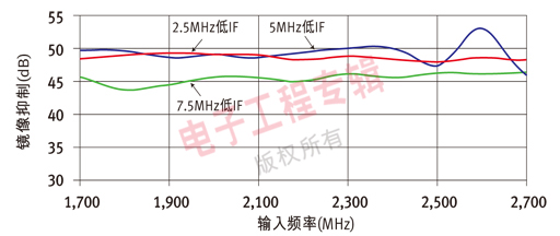
Figure 5: Relationship between W-CDMA image rejection and different IF frequencies.
Polyester Tipped Swabs,Cleanroom Polyester Swab,Sterile Polyester Tipped Applicators,Flat Rectangular Head Swab
Miraclean Technology Co., Ltd. , https://www.mrccleanroom.com