Research on radio frequency interference on UART communication port
A customer reported that the RF interference centered around 840MHz affects the serial communication port configured as a UART. The interface is located between a modem containing an AD6903 (LeMansLCR +) digital baseband processor and a host processor.
The problem is that there is noise in the UARTRX signal connected to the AD6903GPIO_1 pin. Whenever a radio frequency (RF) interference source appears, the average voltage of the signal will be far from its expected value. The average voltage offset depends on the power and frequency of the RF source.
Figure 1 shows the situation where the UARTRX signal on the GPIO_1 pin of the AD6903 is affected when the RF power amplifier is turned on. In Figure 1, the UARTRX entering the AD6903 is represented in pink, the UARTTX signal from the main processor is represented in purple, the power amplifier enable is represented in yellow, and the AD6903VEXT power supply is represented in green.
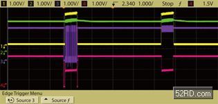
Figure 1: RF interference on the UART communication port
When the power amplifier is turned on (yellow), the UART data transmission from the TX pin of the main processor to the RX pin (pink) of the AD6903 fails because the RX signal rises to the middle position between high and low It is inconsistent with the TX signal (purple). During the second pulse, when the power amplifier is turned on, both the TX pin of the main processor and the RX pin of the AD6903 should remain high; however, there is noise on the TX pin, and the RX signal drops to its high and low power Flat middle position. Also note that the noise on the VEXT supply voltage (green) increases, and its value will rise slightly when the power amplifier is turned on.
However, the problem must be independent of the power amplifier enable signal and the power amplifier of the same modem, because the RF energy from other nearby phones or signal generators will also affect the UARTRX signal entering the AD6903. When using the signal generator scan to check the susceptibility to radio frequency interference, it was found that the worst place was about 840MHz, and it was better at high frequencies or lower.
The series resistor of this signal between the main processor and the AD6903 is used to reduce the logic high level from 3.3V to 2.8V. The rated resistance of this resistor is 10kΩ. It can be replaced with a smaller resistance, including a 0Ω resistor, because lowering the resistance can reduce noise, but this does not solve the problem unless a short-circuit wire is used instead.
This problem is not unique to AD6903. Chips from other manufacturers have a similar phenomenon. For example, SN74AVCA16425GR has the same problem on pin 37. Please refer to Figure 2 for its functional block diagram.
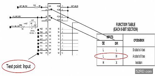
Figure 2: SN74AVCA16425GR functional block diagram
Here 1DIR and 2DIR are high level and OE is low level, so the operation is from port A to port B. Pin 37 (1A7) will receive data from another chipset. This means that it is an input type.
When there is RF interference nearby, that is, near the test point (within 5 meters), use a mobile phone to test the signal on pin 37 of SN74AVCA16425GR. Figure 3 shows that when the device is not powered (I / O status is unknown), its output is abnormal; while Figure 4 shows the device's output when it is powered on (input status).
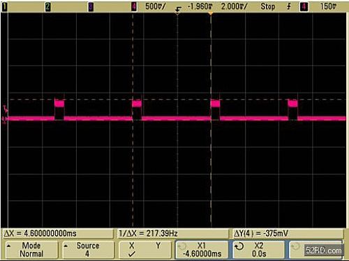
Figure 3: Low level rise
Interference principle
The occurrence of this "RF interference pickup" behavior of the UARTRX signal entering the AD6903 is centered on a specific RF frequency, and these signal traces are not completely shielded. This phenomenon can be explained: the printed wires of the motherboard pick up interference because of the parasitic inductance, parasitic resistance and parasitic capacitance on the wires, and the two ends of the wire are connected with high impedance; one side is a 10kΩ resistor, the other It is a CMOS input. The wire on the circuit board is like an antenna with a 1/4 wavelength response.
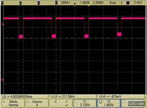
Figure 4: High level reduction
In the customer module, when calculating the GPIO1 wire, the module is calculated as 30mm, while the motherboard is about 15mm. So it is not surprising that this line can pick up RF noise and is sensitive to 840MHz. Refer to Figure 5 for details.

Figure 5: RF interference calculation formula
According to the above theory, it is recommended to add a capacitor on the signal path to damp the RF interference oscillation. The function of the capacitor is to change the tuning frequency of the antenna and reduce the antenna impedance to reduce the antenna gain. Afterwards, we listened to the report, that is, by choosing appropriate capacitors, the noise was reduced to an acceptable level.
The DC offset of this signal can be generated by the diode of any CMOS input-output pin. They are often referred to as ESD (electrostatic discharge) protection diodes, but when it is configured as an output, they are actually used to control the depletion region of the transistor of the pin; those transistors are often used for dual purposes, that is, when configured as input Also acts as an ESD protection device on the pin. So they are indispensable in all CMOS input / output circuit structures. These diodes are forward biased. When the amplitude of the signal causes the diode voltage drop (approximately 0.6V) to exceed VEXT in the forward direction or fall below ground level in the reverse direction, the signal will be clamped. In order to increase the amplitude of the signal as the RF energy in the antenna band increases, the average voltage of the signal will be close to half of the VEXT voltage.
This explanation tells us that the peak-to-peak value of the signal is from VEXT + 0.6V to -0.6V. But the amplitude measured by the oscilloscope is much smaller. To explain why the amplitude is reduced, we estimate that this is due to the attenuation caused by the oscilloscope probe and contact resistance, or the sampling rate of the digital oscilloscope is not enough, for example, it is used to acquire a complete signal near 1GHz (especially given the display window At about 10ms), the actual sampling rate may be much slower than the required 2G samples per second. This theory is described in Figure 6.
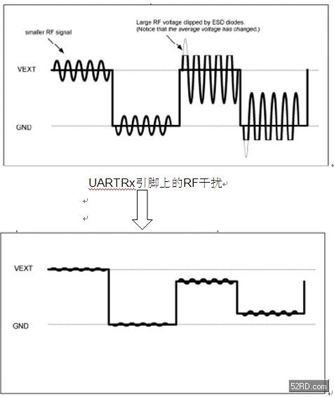
Figure 6: Explanatory description for DC voltage offset observation
The RF interference signal is picked up by the printed wires and fed into the chip. The standard chip input / output attenuator acts as a rectifier and is part of all CMOS input-output pins (chip input / output). The diode is forward biased. And when the forward direction exceeds the diode drop (about 0.6V) above VEXT, or the reverse direction is below ground level, the signal swing is clamped. At the same time, the oscilloscope and / or probe cannot measure the GHz frequency, and its performance is equivalent to a low-pass filter. As a result, abnormal voltages appear on "some" input / output pins (depending on the printed wires connected to the input / output pins and the design level of EMC).
It has also been reported to replace 10kΩ series resistors with 0Ω resistors. This does not eliminate interference or DC level shifts, but it can be achieved by replacing them with short wires. Note that those resistors can be explained. Even 0 ohm resistors will generate parasitic inductance because the package is connected in series with a certain amount of resistance. When considering high frequencies, this series RL component acts more like a low-pass filter than a pure resistor. Therefore, it seems that in the RF band where interference occurs, the resistance component may still have a considerable impedance.
solution
There are two ways to reduce / eliminate the above effects:
1. Eliminate / reduce "interference sources" and increase the system's immunity to immunity (EMC protection), such as isolating RF circuits from other digital circuits, adding independent RF and baseband shielding areas, maintaining good grounding, and using EMC materials in mobile phone cases .
2. In order to remove this "interference", usually a small capacitor should be used (pay attention to the capacitor close to the I / O pin). By adding a 27pf capacitor near the (AD6903.GPIO1) (UART_Rx) test point to ground. It can be found from the oscilloscope measurement that the input / output DC offset is eliminated. And the corresponding bit error rate of the UART communication port is normal. Refer specifically to Figures 7 and 8.
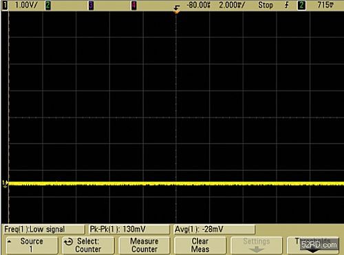
Figure 7: Low-level normal trace.
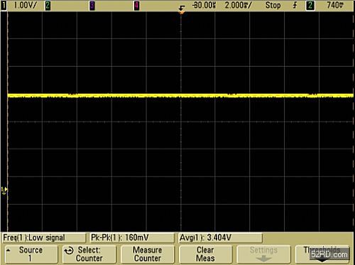
Figure 8: High-level normal trace
This paper address: http: //TIcle/84/119/2010/20100420216399.html
LC1-D series AC Contactor is a kind of econimic products.It can be worked in different quality lever. Big difference for each quality level depend on the raw material and silver contact.This model Magnetic AC Contactor can match any quality level demand in the market. LC1-D series magnetic contactors are exact copy one of the most advanced big company schneider model. The quality and design are most reasonable which certified by the user in the market for a long time.
The magnetic Contactor is suitable for using in the circuits up to the rated voltage 660VAC 50Hz or 60Hz, rated current up to 95A, for making and breaking and frequently start, controlling the AC motor. Combined with the auxiliary contactor group, air delayer, machine interlocking devices etc. It is combined into the delay contactor, mechanical interlocking contactor, start-delta starter, with the Thermal Relay, it is combined into the electromagnetic starter.

Economic AC Contactor,Motor Control Contactor,Industrial Use AC Contactor,Motor Control AC Contactor
Ningbo Bond Industrial Electric Co., Ltd. , https://www.bondelectro.com