Introduction The pulse tester is an electronic instrument used to measure the number of pulse beats of a person, and it is also the main component of the electrocardiogram. Therefore, it has an important role in modern medicine. Although there are many instruments for detecting pulses at present, there are few portable all-digital pulse measuring devices that can realize various functions such as accurate measurement, accurate display and accurate timing function. With the improvement of people's living environment and economic conditions, as well as the improvement of cultural qualities, their lifestyles, health care needs, disease types, and treatment measures have undergone significant changes. However, at present, China's cardiovascular and cerebrovascular diseases are still increasing year by year. Its morbidity and mortality are the first among various diseases and one of the main causes of human death. Therefore, it is necessary to recognize, prevent and detect these diseases early.
Extracting the physiological and pathological information of the human body from the pulse wave as the basis for clinical diagnosis and treatment has always been valued by the Chinese and foreign medical circles. Almost all the nations in the world have used "touching the pulse" as a means of diagnosing diseases. The comprehensive information of the morphology (waveform), intensity (amplitude), velocity (wave velocity) and rhythm (cycle) presented by the pulse wave largely reflects the blood flow characteristics of many physiological pathologies in the human cardiovascular system Therefore, it has high medical value and application prospect for pulse wave collection and processing. However, the biological signals of the human body are mostly low-frequency weak signals in the background of strong noise. The pulse wave signal is a low-frequency weak non-electrophysiological signal, which must be amplified and post-filtered to meet the acquisition requirements.
1 Basic structure module 1.1 Pulse wave detection circuit The current pulse wave detection system has the following detection methods: photoelectric volume pulse wave method, liquid coupled cavity pulse sensor, piezoresistive pulse sensor and strain pulse sensor. In recent years, photoelectric detection technology has developed rapidly in clinical medical applications. This is mainly due to the fact that light energy avoids strong electromagnetic interference, has high insulation, and can non-invasively detect various symptom information of patients. The extraction of fingertip pulse light information by photoelectric method has attracted the attention of experts and scholars working in biomedical instruments. This system has designed a finger-type transmission type photoelectric sensor, which realizes photoelectric isolation and reduces the interference to the subsequent analog circuit.
The sensor is a kind of measuring device that converts the measured into a certain physical quantity with a certain accuracy and is easy to apply. The photoelectric sensor used is composed of a light-emitting diode and a photodiode. Its working principle is: the light emitted by the light-emitting diode transmits through the finger, and the blood passing through the finger tissue is absorbed and attenuated, and is received by the photodiode. Since finger arterial blood shows periodic pulsation changes during blood circulation, its absorption and attenuation of light are also pulsating periodically, so the change of the output signal of the photodiode also reflects the pulsation changes of arterial blood.
1.2 Pulse signal pickup circuit Infrared receiving diode can produce electric energy under the irradiation of infrared light, and a single diode can produce 0.4_V voltage and 0.5mA current. The working wavelength of BPW83 infrared receiving diode and IR333 infrared emitting diode are both 940nm. In the finger clip, infrared receiving diode and infrared emitting diode are placed relatively to obtain the best directivity characteristics. The greater the current in the infrared emitting diode, the smaller the emission angle, and the greater the intensity of the emission. In Figure 1, the selection of 100 Ω for R0 is based on the sensitivity of the infrared light received by the infrared receiving diode. If R0 is too large, the current through the infrared emitting diode is too small, and the PBW83 infrared receiving diode cannot distinguish between the signal with and without pulse. Conversely, if R0 is too small, the passing current is too large, and the infrared receiving diode cannot accurately distinguish between the signal with and without pulse. When the infrared light emitted by the infrared emitting diode directly irradiates the infrared receiving diode, the potential of the inverting input terminal of IC1B is greater than the potential of the in-phase input terminal, and Vi is "0". When the finger is in the measurement position, there are two situations: One is the pulseless period. Although the finger blocks the infrared light emitted by the infrared emitting diode, there is still a dark current of 1 μA due to the dark current in the infrared receiving diode. The Vi potential is slightly lower than 2.5V. Second, there is a pulse period. When there is a beating pulse, the blood pulse deteriorates the light transmittance of the finger, the dark current in the infrared receiving diode decreases, and the Vi potential rises.
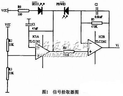
1.3 Signal acquisition and processing system Because the photoelectric pulse wave is a weak physiological signal that changes slowly, the signal-to-noise ratio is low, and it is extremely susceptible to interference from environmental noise and limb movement. The traditional photoelectric pulse wave signal detection circuit uses a high gain amplifier to obtain higher detection sensitivity. This design idea leads to a reduction in the dynamic range of the detection signal. When it is interfered by motion, it will cause photoelectricity due to the interference signal. Saturation distortion detected by pulse wave signal. This system uses oversampling technology to improve the sampling accuracy by high-speed sampling of the signal, which is equivalent to analog-to-digital conversion of the signal with a high-resolution ADC to achieve the effect of improving the signal-to-noise ratio and improving the dynamic range. Therefore, this system performs analog-to-digital conversion on the signal after photoelectric conversion without any signal conditioning (amplification and filtering) circuit.
1.4 Application of oversampling technology The so-called oversampling technology refers to the method of sampling analog signals at a frequency much higher than the Nyquist sampling frequency. According to the theory of signal sampling and quantization, if the minimum amplitude of the input signal is greater than the quantization level of the quantizer and the amplitude of the input signal is randomly distributed, the total power of the quantization noise is a constant, evenly distributed in the frequency range of 0 to fs. Therefore, the quantization noise level is inversely proportional to the sampling frequency. If the sampling frequency is increased, the quantization noise level can be reduced. Since the baseband is fixed, the noise power in the baseband range is reduced, and the signal-to-noise ratio is improved. Increase the resolution, and every time the sampling frequency is increased by 4 times, the signal-to-noise ratio is increased by 4 times, which is equivalent to the resolution of A / D increased by 1 bit.
2 software design 2.1 program design This article selects the single chip ADC841 of ADI Company, which integrates a 12-bit successive approximation ADC with a speed of up to 400k and a resolution of 0.6mv / LSB. Starting from the software requirements and the speed of the single-chip microcomputer, the ADC sampling rate fs is set to 102.4kHz. For ease of calculation, the oversampling multiple k is set to 64, then the sampling rate after the down-extraction is pseudo: fs / k = 1600Hz, which is Four times the 400 Hz carrier, satisfying the Nyquist sampling theorem. Since the oversampling multiple k is 64, it can be calculated by increasing the resolution by one bit every time the sampling rate is increased by 4 times. The effective resolution of the obtained ADC can be increased by 3 bits, and finally it can achieve an accuracy of about 15 bits. .0763mv / LSB. Set ADCCON1 = # 0B2H, ADCCON2 = # 00H. Timer 2 is a timer with 16-bit auto-reload function. When used as a timer, TH2 and TL2 count the number of machine cycles. The automatic reload of the contents of TH2 and TL2 is implemented through registers RCAP2H and RCAP2L. All four registers are initialized and the auto-load value is # 0FFCAH.
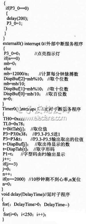
2.2 Program source code

3 Conclusion The analog circuit of this system is simple. The ADC841 chip implements functions such as pulse signal acquisition, signal processing and pulse frequency calculation. Therefore, it has small size, low power consumption and high system stability. The system can realize real-time storage of pulse wave and real-time communication with the host computer (PC), so it can be used as a module of the multi-parameter patient central monitoring system to complete heart rate detection and pulse waveform display.
Our Driverless LED Street Light Use Seoul IC drive program, driverless, ultra-high efficiency 125LM / W, PF> 0.9, no EMI electromagnetic interference, 10KV Surge Protection, more than 50000 hours lifespan, 5 years warranty, Mainly used for To be installed in the garden, residential area, Road, Highway, courtyard, etc. Available in 40W, 50W, 100W, 150W, 200W, versions.
Driverless LED Street Light
Driverless LED Street Light,LED Street Light,LED Street Light Driverless,LED Street Lighting
Shenzhen Ri Yue Guang Hua Technology Co., Ltd. , https://www.ledlightinside.com